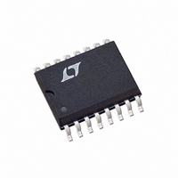
LTC1625IS Linear Technology, LTC1625IS Datasheet

LTC1625IS
Specifications of LTC1625IS
Available stocks
Related parts for LTC1625IS
LTC1625IS Summary of contents
Page 1
... RUN/SS pin provides soft start capability for supply sequencing. A wide supply range allows operation from 3.7V (3.9V for LTC1625I) to 36V at the input and 1.19V LTC and LT are registered trademarks of Linear Technology Corporation and Burst Mode are trademarks of Linear Technology Corporation. SENSE ...
Page 2
... Pin Open OSENSE PROG C = 3300pF LOAD C = 3300pF LOAD U W ORDER PART TOP VIEW NUMBER LTC1625CGN LTC1625CS LTC1625IGN LTC1625IS 12 5 BOOST 11 6 INTV PGND S PACKAGE 16-LEAD PLASTIC SO = 130 C/W (GN 110 C/W (S) JA MIN TYP MAX 10 50 1.178 1.190 1.202 3.220 3.300 3.380 4 ...
Page 3
... Note 1: Absolute Maximum Ratings are those values beyond which the life of a device may be impaired. Note calculated from the ambient temperature T J dissipation P according to the following formula: D LTC1625CGN/LTC1625IGN • 130 C/ LTC1625CS/LTC1625IS • 110 C/ 15V unless otherwise noted CONDITIONS C = 3300pF LOAD ...
Page 4
LTC1625 W U TYPICAL PERFOR A CE CHARACTERISTICS Efficiency vs Load Current 100 BURST MODE 90 OPERATION CONTINUOUS MODE 10V OUT EXTV = V CC OUT 50 0.001 0.01 0.1 1 ...
Page 5
W U TYPICAL PERFOR A CE CHARACTERISTICS Maximum Current Sense Voltage vs Duty Cycle 200 150 100 0.2 0.4 0.5 0.8 DUTY CYCLE 1625 G10 FCB Pin Current vs Temperature 0 – 0.25 – 0.50 – 0.75 ...
Page 6
LTC1625 PIN FUNCTIONS EXTV (Pin 1): INTV Switch Input. When the EXTV CC CC voltage is above 4.7V, the switch closes and supplies INTV power from EXTV . Do not exceed 7V at this pin ...
Page 7
U U FUNCTIONAL DIAGRA THB – 0. – 1.19V 0.6V – RUN/ – 1.28V OV ...
Page 8
LTC1625 U OPERATIO Main Control Loop The LTC1625 is a constant frequency, current mode controller for DC/DC step-down converters. In normal operation, the top MOSFET is turned on when the RS latch is set by the on-chip oscillator and is ...
Page 9
U U APPLICATIONS INFORMATION The basic LTC1625 application circuit is shown in Figure 1. External component selection is primarily determined by the maximum load current and begins with the selection of the sense resistance and power MOSFETs. Because the LTC1625 ...
Page 10
LTC1625 U U APPLICATIONS INFORMATION V OUT Top Duty Cycle – OUT Bottom Duty Cycle V IN The MOSFET power dissipations at maximum output current are OUT TOP O ...
Page 11
U U APPLICATIONS INFORMATION The corresponding average current depends on the amount of ripple current. Lower inductor values (higher I reduce the load current at which Burst Mode operation begins. The output voltage ripple can increase during Burst Mode operation ...
Page 12
LTC1625 U U APPLICATIONS INFORMATION Ferrite designs have very low core loss and are preferred at high switching frequencies, so design goals can con- centrate on copper loss and preventing saturation. Ferrite core material saturates “hard,” which means that induc- ...
Page 13
U U APPLICATIONS INFORMATION High input voltage applications in which large MOSFETs are being driven at high frequencies may cause the LTC1625 to exceed its maximum junction temperature rating. Most of the supply current drives the MOSFET gates unless an ...
Page 14
LTC1625 U U APPLICATIONS INFORMATION Note that R also varies with the gate drive level. If DS(ON) gate drives other than the 5.2V INTV be accounted for when selecting the MOSFET R Particular care should be taken with applications where ...
Page 15
U U APPLICATIONS INFORMATION DELAY When the voltage on RUN/SS reaches 1.4V the LTC1625 begins operating with a clamp on I voltage on RUN/SS increases to ...
Page 16
LTC1625 U U APPLICATIONS INFORMATION where L1, L2, etc. are the individual losses as a percentage of input power often useful to analyze individual losses to determine what is limiting the efficiency and which change would produce the ...
Page 17
U U APPLICATIONS INFORMATION automobile is the source of a number of nasty potential transients, including load dump, reverse and double battery. Load dump is the result of a loose battery cable. When the cable breaks connection, the field collapse ...
Page 18
LTC1625 U U APPLICATIONS INFORMATION 1 EXTV 0.1 F INTV SYNC CC 3 RUN/ 470pF C OPEN FCB 10k 220pF 6 SGND AVX ...
Page 19
U U APPLICATIONS INFORMATION OPTIONAL 5V EXTV CC CONNECTION EXT C SS CLK OPEN OPEN R1 OUTPUT DIVIDER REQUIRED WITH V OPEN PROG BOLD LINES INDICATE HIGH CURRENT PATHS U TYPICAL APPLICATIONS ...
Page 20
LTC1625 U TYPICAL APPLICATIONS 1 EXTV 0.1 F SYNC 3 RUN/ LTC1625 4 R 1nF C OPEN FCB 10k 330pF 6 SGND 7 V OSENSE 8 V OPEN PROG ...
Page 21
U TYPICAL APPLICATIONS 3.3V/4A Fixed Output with 12V/120mA Auxiliary Output 1 EXTV EXT 0.1 F SYNC CLK 3 RUN/SS LTC1625 FCB 10k 5 I BOOST 220pF 470pF 6 ...
Page 22
LTC1625 U TYPICAL APPLICATIONS 2.2nF SS C 0.1 F 10k C C2 220pF C : SANYO 16SV220M SANYO 6SV470M OUT L1: MAGNETICS Kool-M 77120-A7, 9 TURNS, 17 GAUGE 1 EXTV ...
Page 23
... FLASH SHALL NOT EXCEED 0.010" (0.254mm) PER SIDE Information furnished by Linear Technology Corporation is believed to be accurate and reliable. However, no responsibility is assumed for its use. Linear Technology Corporation makes no represen- tation that the interconnection of its circuits as described herein will not infringe on existing patent rights. ...
Page 24
... Frequency Ideal for 5V to 3.3V 5V Standby Output and Auxiliary Linear Regulator 2. Input, 90% Efficiency, Ideal for 3.3V to 1.xV – 2. 20A 28V 35V OUT 3.3V 1.8A C OUT + 100 F 10V 0 MBRS140T3 1625 TA07 Saves Space, Fixed SENSE 1625f LT/TP 1298 4K • PRINTED IN USA LINEAR TECHNOLOGY CORPORATION 1998 ...


