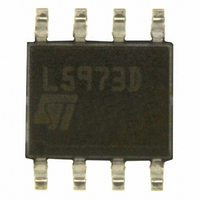
L5973D013TR STMicroelectronics, L5973D013TR Datasheet

L5973D013TR
Specifications of L5973D013TR
E-L5973D013TR
Available stocks
Related parts for L5973D013TR
L5973D013TR Summary of contents
Page 1
Features ■ 2.5 A internal switch ■ Operating input voltage from ■ 3 (±2%) reference voltage ■ Output voltage adjustable from 1.235 ■ Low dropout operation: 100 % duty ...
Page 2
Contents Contents 1 Pin settings . . . . . . . . . . . . . . . . . . . . . . . . . . . . . . . . . . . ...
Page 3
L5973D 1 Pin settings 1.1 Pin connection Figure 2. Pin connection (top view) 1.2 Pin description Table 1. Pin description N° Type 1 OUT 2 SYNC 3 INH 4 COMP VREF 7 GND 8 VCC OUT 1 ...
Page 4
Electrical data 2 Electrical data 2.1 Maximum ratings Table 2. Absolute maximum ratings Symbol V Input voltage 8 Output DC voltage V 1 Output peak voltage 0.1 µs I Maximum output current Analog ...
Page 5
L5973D 3 Electrical characteristics Table 4. Electrical characteristics ( ° Symbol Operating input V CC voltage range Mosfet on R DS(on) Resistance Maximum limiting I l current f Switching frequency s Duty cycle Dynamic characteristics ...
Page 6
Electrical characteristics Table 4. Electrical characteristics (continued ° Symbol I Source bias current b DC open loop gain gm Transconductance Sync function High input voltage Low input voltage Slave sink current Master output amplitude ...
Page 7
L5973D 4 Typical characteristics Figure 3. Line regulation Vo (V) 3.312 Vcc = 12V 3.308 Vo = 3.3V 3.304 3.3 3.296 3.292 3.288 3.284 3.28 3.276 0 10 Figure 5. Output voltage vs junction temperature Vo (V) 1.25 1.24 1.23 ...
Page 8
Typical characteristics Figure 8. Junction temperature vs output current Tj(°C) 120 110 Vin=5V 100 Tamb=25° 0.2 0.4 0.6 0.8 1 1.2 1.4 1.6 1.8 2 2.2 2.4 2.6 Figure 10. Efficiency vs ...
Page 9
L5973D 5 Application circuit In figure 6 is shown the demonstration board application circuit, where the input supply voltage can range from due to the rated voltage of the input capacitor and CC ...
Page 10
Application circuit Figure 13. PCB layout (component side) Figure 14. PCB layout (bottom side) Figure 15. PCB layout (front side) Below some graphs show the T output voltage and some efficiency measurements. 10/17 versus output current in different conditions of ...
Page 11
L5973D 6 Application ideas Figure 16. Positive buck-boost regulator Figure 17. Buck-boost regulator Figure 18. Dual output voltage with auxiliary winding Application ideas 11/17 ...
Page 12
Application ideas When an output voltage below the internal reference (1.235 V) is required, the circuit reported in the figure 18 can been used. In this case the minimum voltage reachable is 0.6 V and can be easily calculated with ...
Page 13
L5973D 7 Package mechanical data In order to meet environmental requirements, ST offers these devices in ECOPACK® packages. These packages have a Lead-free second level interconnect . The category of second level interconnect is marked on the package and on ...
Page 14
Package mechanical data Table 6. HSOP8 mechanical data Dim ccc Figure 20. Package dimensions 14/17 mm Min Typ Max 1.70 0.00 0.10 1.25 0.31 0.51 0.17 ...
Page 15
... L5973D 8 Order code Table 7. Order code Part number L5973D L5973D013TR Package HSOP8 (Exposed pad) HSOP8 (Exposed pad) Order code Packaging Tube Tape and reel 15/17 ...
Page 16
Revision history 9 Revision history pp Table 8. Revision history Date 01-Nov-2005 22-May-2006 13-Nov-2006 26-Jan-2007 17-Oct-2007 24-Oct-2007 07-Jan-2008 16/17 Revision 10 Updated package information Electrical characteristic 11 Figure 19 added, new template 12 Typo in order codes 13 Updated Table ...
Page 17
... L5973D Information in this document is provided solely in connection with ST products. STMicroelectronics NV and its subsidiaries (“ST”) reserve the right to make changes, corrections, modifications or improvements, to this document, and the products and services described herein at any time, without notice. All ST products are sold pursuant to ST’s terms and conditions of sale. ...


