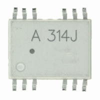
HCPL-314J-000E Avago Technologies US Inc., HCPL-314J-000E Datasheet

HCPL-314J-000E
Specifications of HCPL-314J-000E
Available stocks
Related parts for HCPL-314J-000E
HCPL-314J-000E Summary of contents
Page 1
... RoHS 6 fully compliant options available; -xxxE denotes a lead-free product Description The HCPL-314J family of devices consists of an Al- GaAs LED optically coupled to an integrated circuit with a power output stage. These optocouplers are ideally suited for driving power IGBTs and MOSFETs used in motor control inverter applications. The high operating voltage range of the output stage provides the drive voltages required by gate controlled devices ...
Page 2
... HCPL-314J-500E to order product of SO-16 Surface Mount package in Tape and Reel packaging with IEC/EN/ DIN EN 60747-5-2 Safety Approval in RoHS compliant. Example 2: HCPL-314J to order product of SO-16 Surface Mount package in tube packaging with IEC/EN/DIN EN 60747- 5-2 Safety Approval and non RoHS compliant. Option datasheets are available. Contact your Avago sales representative or authorized distributor for information. ...
Page 3
... Recommended Pb-Free IR Profile Recommended reflow condition as per JEDEC Standard, J-STD-020 (latest revision). Non-Halide Flux should be used. Regulatory Information The HCPL-314J has been approved by the following organizations: IEC/EN/DIN EN 60747-5-2 Approved under: IEC 60747-5-5:1997 + A1:2002 EN 60747-5-2:2001 + A1:2002 DIN EN 60747-5-2 (VDE 0884 Teil 2):2003-01. ...
Page 4
... Input Power Dissipation Lead Solder Temperature Solder Reflow Temperature Profile Recommended Operating Conditions Parameter Power Supply Input Current (ON) Input Voltage (OFF) Operating Temperature 4 HCPL-314J Units Conditions 8.3 mm Measured from input terminals to output terminals, shortest distance through air. 8.3 mm Measured from input terminals to output terminals, shortest distance path along body ...
Page 5
Electrical Specifications (DC) Over recommended operating conditions unless otherwise specified. Parameter Symbol High Level Output Current I OH Low Level Output Current I OL High Level Output Voltage V OH Low Level Output Voltage V OL High Level Supply Current ...
Page 6
... OH 7. Maximum pulse width = 1 ms, maximum duty cycle = 20 accordance with UL 1577, each HCPL-314J optocoupler is proof tested by applying an insulation test voltage ≥ 6000 V This test is performed before 100% production test for partial discharge (method B) shown in the IEC/EN/DIN EN 60747-5-2 Insulation Char- acteristics Table, if applicable. ...
Page 7
T – TEMPERATURE – °C A Figure 1. V vs. Temperature. OH 0.44 0.43 0.42 0.41 0.40 0.39 -50 - 100 125 ...
Page 8
T PLH T PHL – SUPPLY VOLTAGE – Figure 10. Propagation Delay vs 400 350 T PLH 300 T PHL 250 200 0 50 ...
Page 9
500 Ω + – 10 KHz 50% DUTY 3 CYCLE 4 Figure 17. Propagation Delay Test Circuit and Waveforms – ...
Page 10
... Applications Information Eliminating Negative IGBT Gate Drive To keep the IGBT firmly off, the HCPL-314J has a very low maximum V specification of 1.0 V. Minimizing Rg and OL the lead inductance from the HCPL-314J to the IGBT gate and emitter (possibly by mounting the HCPL-314J on a small PC board directly above the IGBT) can eliminate the need for negative IGBT gate drive in many applica- tions as shown in Figure 19 ...
Page 11
... HCPL-314J. V – ≥ I OLPEAK 24 V – 0. Ω The V value the previous equation is the 0.6A. (See Figure 6). Step 2: Check the HCPL-314J power dissipation and increase Rg if necessary. The HCPL-314J total power dissipation (P ter power (P ) and the output power ( Duty Cycle ...
Page 12
C LEDP LEDN 4 5 Figure 21. Optocoupler Input to Output Capacitance Model for Unshielded Optocouplers LEDP LEDP SAT – LEDN 4 SHIELD ...
Page 13
... Figure 27. The maxi- mum dead time for the HCPL-314J is 1 μs (= 0.5 μs - (-0.5 μs)) over the operating temperature range of - 40°C to 100°C. Note that the propagation delays used to calculate PDD ...
Page 14
I LED1 V OUT1 OFF V OUT2 I LED2 t PHL MAX PDD* MAX = (t *PDD = PROPAGATION DELAY DIFFERENCE NOTE: FOR PDD CALCULATIONS THE PROPAGATION DELAYS ARE TAKEN AT THE SAME TEMPERATURE AND TEST CONDITIONS. ...


