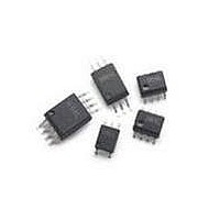
ACPL-M61L-060E Avago Technologies US Inc., ACPL-M61L-060E Datasheet - Page 6

ACPL-M61L-060E
Manufacturer Part Number
ACPL-M61L-060E
Description
OPTOCOUPLER 10MBD ULP 5-SOIC
Manufacturer
Avago Technologies US Inc.
Series
R²Coupler™r
Datasheet
1.ACPL-M61L-500E.pdf
(17 pages)
Specifications of ACPL-M61L-060E
Package / Case
6-SOIC (0.173", 4.40mm Width) 5 Leads
Voltage - Isolation
3750Vrms
Number Of Channels
1, Unidirectional
Current - Output / Channel
10mA
Data Rate
10MBd
Propagation Delay High - Low @ If
46ns @ 6.5mA
Current - Dc Forward (if)
8mA
Input Type
DC
Output Type
Push-Pull, Totem-Pole
Mounting Type
Surface Mount
Isolation Voltage
3750 Vrms
Maximum Fall Time
12 ns
Maximum Rise Time
12 ns
Output Device
Logic Gate Photo IC
Configuration
1 Channel
Maximum Baud Rate
10 MBps
Maximum Forward Diode Voltage
6.5 V
Maximum Reverse Diode Voltage
5 V
Maximum Power Dissipation
20 mW
Maximum Operating Temperature
+ 105 C
Minimum Operating Temperature
- 40 C
No. Of Channels
1
Optocoupler Output Type
Logic Gate
Input Current
150mA
Output Voltage
7V
Opto Case Style
SOIC
No. Of Pins
5
Peak Reflow Compatible (260 C)
Yes
Rohs Compliant
Yes
Number Of Elements
1
Forward Voltage
1.7V
Forward Current
8mA
Output Current
10mA
Operating Temp Range
-40C to 105C
Pin Count
5
Mounting
Surface Mount
Reverse Breakdown Voltage
5V
Operating Temperature Classification
Industrial
Leaded Process Compatible
Yes
Lead Free Status / RoHS Status
Lead free / RoHS Compliant
Lead Free Status / RoHS Status
Lead free / RoHS Compliant, Lead free / RoHS Compliant
Available stocks
Company
Part Number
Manufacturer
Quantity
Price
Part Number:
ACPL-M61L-060E
Manufacturer:
AVAGO/安华高
Quantity:
20 000
IEC/EN/DIN EN 60747-5-5 Insulation Characteristics* (Option 060)
*
** Refer to the following figure for dependence of P
Absolute Maximum Ratings
6
Description
Installation classification per DIN VDE 0110/39, Table 1
Climatic Classification
Pollution Degree (DIN VDE 0110/39)
Maximum Working Insulation Voltage
Input to Output Test Voltage, Method b*
V
Partial discharge < 5 pC
Input to Output Test Voltage, Method a*
V
Partial discharge < 5 pC
Highest Allowable Overvoltage
(Transient Overvoltage t
Safety-limiting values
– maximum values allowed in the event of a failure.
Insulation Resistance at T
Parameter
Storage Temperature
Operating Temperature
Reverse Input Voltage
Supply Voltage
Average Forward Input Current
Peak Forward Input Current
(I
Output Current
Output Voltage
Input Power Dissipation
Output Power Dissipation
Lead Solder Temperature
Solder Reflow Temperature Profile
F
IORM
IORM
Refer to the optocoupler section of the Isolation and Control Components Designer’s Catalog, under Product Safety Regulations section, (IEC/EN/
DIN EN 60747-5-5) for a detailed description of Method a and Method b partial discharge test profiles.
at 1 Ps pulse width, <10% duty cycle)
for rated mains voltage ≤ 150 V
for rated mains voltage ≤ 300 V
for rated mains voltage ≤ 600 V
for rated mains voltage ≤ 1000 V
Case Temperature
Input Current**
Output Power**
x 1.875=V
x 1.6=V
PR
, Type and Sample Test, t
PR
, 100% Production Test with t
ini
S
, V
= 60 sec)
IO
= 500 V
rms
rms
rms
rms
m
= 10 sec,
Symbol
T
T
V
V
I
I
I
V
P
P
T
See Package Outline Drawings section
F
F(TRAN)
O
A
S
LS
R
DD
O
I
O
S
m
and I
=1 sec,
S
on ambient temperature.
Min
-55
-40
–
–
–0.5
Symbol
V
V
V
V
T
I
P
R
S, INPUT
S
S, OUTPUT
IORM
PR
PR
IOTM
S
Max
125
105
5
6.5
8
1
80
10
V
14
20
260°C for 10 sec., 1.6 mm below seating plane
DD
+0.5
ACPL-061L^/
ACPL-064L/
55/105/21
ACPL-M61L
1063
6000
I – IV
>10
I – III
I – II
560
896
150
150
600
2
9
Characteristic
Units
°C
°C
V
V
mA
A
mA
mA
V
mW
mW
ACPL-W61L/
55/105/21
ACPL-K64L
Condition
≤1 Ps Pulse Width,
<300 pulses per second
≤1 Ps Pulse Width,
<10% Duty Cycle
I – IV
I – IV
1140
2137
1824
8000
>10
I – III
I – III
175
230
600
2
9
Unit
V
V
V
V
°C
mA
mW
:
peak
peak
peak
peak


