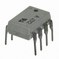
HCPL-J312-000E Avago Technologies US Inc., HCPL-J312-000E Datasheet - Page 19

HCPL-J312-000E
Manufacturer Part Number
HCPL-J312-000E
Description
OPTOCOUPLER 1CH 2.5A 8-DIP
Manufacturer
Avago Technologies US Inc.
Datasheet
1.HCPL-3120-500E.pdf
(24 pages)
Specifications of HCPL-J312-000E
Output Type
Gate Driver
Package / Case
8-DIP (0.300", 7.62mm)
Voltage - Isolation
3750Vrms
Number Of Channels
1, Unidirectional
Current - Output / Channel
2.5A
Propagation Delay High - Low @ If
300ns @ 7mA ~ 16mA
Current - Dc Forward (if)
16mA
Input Type
DC
Mounting Type
Through Hole
Configuration
1 Channel
Isolation Voltage
3750 Vrms
Maximum Propagation Delay Time
500 ns
Maximum Forward Diode Voltage
1.95 V
Minimum Forward Diode Voltage
1.2 V
Maximum Reverse Diode Voltage
3 V
Maximum Forward Diode Current
25 mA
Maximum Power Dissipation
295 mW
Maximum Operating Temperature
+ 100 C
Minimum Operating Temperature
- 40 C
No. Of Channels
1
Optocoupler Output Type
Gate Drive
Input Current
16mA
Output Voltage
30V
Opto Case Style
DIP
No. Of Pins
8
Common Mode Ratio
15 KV/uS
Rohs Compliant
Yes
Lead Free Status / RoHS Status
Lead free / RoHS Compliant
Lead Free Status / RoHS Status
Lead free / RoHS Compliant, Lead free / RoHS Compliant
Other names
516-1879-5
HCPL-J312-000E
HCPL-J312-000E
Available stocks
Company
Part Number
Manufacturer
Quantity
Price
Company:
Part Number:
HCPL-J312-000E
Manufacturer:
AVAGO
Quantity:
2 000
Part Number:
HCPL-J312-000E
Manufacturer:
AVAGO/安华高
Quantity:
20 000
Figure 26. HCPL-3120 typical application circuit with negative IGBT gate drive.
Selecting the Gate Resistor (Rg) to Minimize IGBT
Switching Losses. (Discussion applies to HCPL-3120,
HCPL-J312 and HCNW3120)
Step 1: Calculate Rg Minimum from the I
tion. The IGBT and Rg in Figure 26 can be analyzed as a
simple RC circuit with a voltage supplied by the HCPL-
3120.
Rg ≥ ———————
The V
servative value of V
Figure 6). At lower Rg values the voltage supplied by
the HCPL-3120 is not an ideal voltage step. This results
in lower peak currents (more margin) than predicted by
this analysis. When negative gate drive is not used V
the previous equation is equal to zero volts.
Step 2: Check the HCPL-3120 Power Dissipation and
Increase Rg if Necessary. The HCPL-3120 total power
dissipation (P
(P
P
PE = I
P
= I
CONTROL
19
T
O
COLLECTOR
E
= P
= P
) and the output power (P
INPUT
= ———————
= ———————
= 7.2 Ω @ 8 Ω
F
CC
OL
+5 V
E
O(BIAS)
74XXX
• V
+ P
OPEN
• (V
value of 2 V in the previous equation is a con-
(V
I
(V
I
(15 V + 5 V - 2 V)
F
CC
CC
O
· Duty Cycle
CC
2.5 A
+ P
– V
– V
T
OLPEAK
270 Ω
OLPEAK
- V
) is equal to the sum of the emitter power
O (SWITCHING)
EE
EE
EE
- V
- 2 V)
)+ E
OL
OL
at the peak current of 2.5A (see
SW
)
(R
1
2
3
4
G
O
, Q
):
G
) • f
HCPL-3120
OL
Peak Specifica-
HCPL-3120 fig 26
8
7
6
5
0.1 µF
EE
in
For the circuit in Figure 26 with I
16 mA, Rg = 8 Ω, Max Duty Cycle = 80%, Qg = 500 nC,
f = 20 kHz and T
P
P
= 85 mW + 104 mW
= 189 mW > 178 mW (P
= 250 mW
The value of 4.25 mA for I
obtained by derating the I
at -40°C) to I
Since P
increased to reduce the HCPL-3120 power dissipation.
P
= P
= 178 mW - 85 mW
= 93 mW
E
For Qg = 500 nC, from Figure 27, a value of E
gives a Rg = 10.3 Ω.
O(SWITCHING MAX)
E
O
SW(MAX)
+
–
+
–
= 16 mA • 1.8 V •
= 4.25 mA • 20 V + 5.2 µ J •
V
V
CC
EE
Rg
O(MAX)
= 15 V
= -5 V
O
for this case is greater than P
Q1
Q2
- P
CC
P
= ———————
f
93 mW
= ———— = 4.65 µW
20 kHz
-
15C*4.8 mW/C)
max at 85C (see Figure 7).
A
O(BIAS)
max = 85 °C:
O(SWITCHINGMAX)
0.8 = 23 mW
CC
O(MAX)
CC
in the previous equation was
max of 5 mA (which occurs
20 kHz
@ 85°C
3-PHASE
+ HVDC
- HVDC
AC
O(MAX)
F
(worst case) =
SW
, Rg must be
= 4.65 µW


