DS1985-F5+ Maxim Integrated Products, DS1985-F5+ Datasheet
DS1985-F5+
Specifications of DS1985-F5+


Related parts for DS1985-F5+


DS1985-F5+ Summary of contents
Page 1
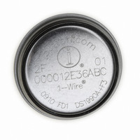
... Easily affixed with self-stick adhesive backing, latched by its flange, or locked with a ring pressed onto its rim Presence detector acknowledges when reader first applies voltage ORDERING INFORMATION PART DS1985-F3+ DS1985-F5+ +Denotes a lead(Pb)-free/RoHS-compliant package EXAMPLES OF ACCESSORIES DS9096P Self-Stick Adhesive Pad DS9101 Multi-Purpose Clip DS9093RA ...
Page 2
... The protocol required for these ROM Function Commands is described in Figure 8. After a ROM Function Command is successfully executed, the memory functions that operate on the EPROM portions of the DS1985 become accessible and the bus master may issue any one of the Figure 8. After a ROM Function Command is successfully executed, the memory functions that operate on the EPROM portions of the DS1985 become accessible and the bus master may issue any one of the five Memory Function Commands specific to the DS1985 to read or program the various data fields ...
Page 3
... DS1985 BLOCK DIAGRAM Figure 1 64-BIT LASERED ROM Each DS1985 contains a unique ROM code that is 64 bits long. The first 8 bits are a 1-Wire family code. The next 48 bits are a unique serial number. The last 8 bits are a CRC of the first 56 bits. (See Figure 3.) The 64-bit ROM and ROM Function Control section allow the DS1985 to operate as a 1-Wire device and follow the 1-Wire protocol detailed in the section “ ...
Page 4
HIERARCHICAL STRUCTURE FOR 1-WIRE PROTOCOL Figure 2 64-BIT LASERED ROM Figure 3 8-Bit CRC Code MSB 48- Bit Serial Number LSB MSB 8-Bit Family Code (0BH) LSB MSB LSB ...
Page 5
... Therefore not possible to simply rewrite a page if the data requires changing or updating, but with space permitting, an entire page of data can be redirected to another page within the DS1985 by writing the one’s complement of the new page address into the Page Address Redirection Byte that corresponds to the original (replaced) page. ...
Page 6
... Redirection Byte. A value of FDH in the redirection byte for page 1, for example, would indicate that the updated data is now in page 2. The details for reading and programming the EPROM status memory portion of the DS1985 are given in the Memory Function Commands section. DS 1985 MEMORY MAP Figure 4 ...
Page 7
... To execute a read sequence, the starting address is issued by the bus master and data is read from the part beginning at that initial location and continuing to the end of the selected data field or until a reset sequence is issued. All bits transferred to the DS1985 and received back by the bus master are sent least significant bit first. ...
Page 8
... With every subsequent read data time slot the bus master receives data from the DS1985 starting at the supplied address and continuing until the end of an 8-byte page of the EPROM Status data field is reached. At that point the bus master will receive a 16-bit CRC of the command byte, address bytes and status data bytes ...
Page 9
MEMORY FUNCTION FLOW CHART Figure ...
Page 10
MEMORY FUNCTION FLOW CHART (cont’d) Figure ...
Page 11
MEMORY FUNCTION FLOW CHART (cont’d) Figure ...
Page 12
... Byte associated with the page given by the starting address. With the next sixteen read data time slots, the bus master receives a 16-bit CRC of the command byte, address bytes and the Redirection Byte. This CRC is computed by the DS1985 and read back by the bus master to check if the command word, starting address and Redirection Byte were received correctly. ...
Page 13
... As the DS1985 receives this byte of data into the scratchpad, it also shifts the data into the CRC generator that has been preloaded with the current address and the result is a 16-bit CRC of the new data byte and the new address ...
Page 14
... For both of these cases, the decision to continue (to apply a Program Pulse to the DS1985) is made entirely by the bus master, since the DS1985 will not be able to determine if the 16-bit CRC calculated by the bus master agrees with the 16-bit CRC calculated by the DS1985 incorrect CRC is ignored and a Program Pulse is applied by the bus master, incorrect programming could occur within the DS1985 ...
Page 15
... For both of these cases, the decision to continue (to apply a Program Pulse to the DS1985) is made entirely by the bus master, since the DS1985 will not be able to determine if the 16-bit CRC calculated by the bus master agrees with the 16-bit CRC calculated by the DS1985 incorrect CRC is ignored and a Program Pulse is applied by the bus master, incorrect programming could occur within the DS1985 ...
Page 16
... This command allows the bus master to read the DS1985’s 8-bit family code, unique 48-bit serial number, and 8-bit CRC. This command can be used only if there is a single DS1985 on the bus. If more than one slave is present on the bus, a data collision will occur when all slaves try to transmit at the same time (open drain will produce a wired-AND result) ...
Page 17
... DS1985 EQUIVALENT CIRCUIT Figure 6 BUS MASTER CIRCUIT Figure 7 CAPACITOR ADDED TO REDUCE COUPLING ON DATA LINE DUE TO PROGRAMMING SIGNAL SWITCHING VP0300L OR VP0106N3 OR BSS110 TO DATA CONNECTION OF DS2505 ...
Page 18
ROM FUNCTIONS FLOW CHART Figure 8 (See Figure ...
Page 19
... DS1985. During write time slots, the delay circuit determines when the DS1985 will sample the data line. For a read data time slot “ 0 “ transmitted, the delay circuit determines how long the DS1985 will hold the data line low overriding the 1 generated by the master. If the data bit is a “ ...
Page 20
... Note that due to the high voltage programming requirements for any 1-Wire EPROM device not possible to multidrop non-EPROM based 1-Wire devices with the DS1985 during programming. An internal diode within the non-EPROM based 1-Wire devices will attempt to clamp the data line at approximately 8 volts and could potentially damage these devices. ...
Page 21
... READ/WRITE TIMING DIAGRAM (cont’d) Figure 10 Write-0 Time Slot Read-Data Time Slot RESISTOR MASTER DS1985 60 s t < 120 s < t LOW0 SLOT 1 s t < REC 60 s t < 120 s SLOT 1 s t < 15 s LOWR 0 t < 45 s RELEASE 1 ...
Page 22
... ROM. The bus master can compute a CRC value from the first 56 bits of the 64-bit ROM and compare it to the value stored within the DS1985 to determine if the ROM data has been received error-free by the bus master. The equivalent polynomial ...
Page 23
... There is no circuitry on the DS1985 that prevents a command sequence from proceeding if the CRC stored in or calculated by the DS1985 does not match the value generated by the bus master. For more details on generating CRC values including example implementations in both hardware and software, see the Book of DS19xx iButton Standards ...
Page 24
ABSOLUTE MAXIMUM RATINGS* Voltage on any Pin Relative to Ground Operating Temperature Storage Temperature This is a stress rating only and functional operation of the device at these or any other conditions outside those indicated in the operation sections ...
Page 25
NOTES: 1. All voltages are referenced to ground external pullup voltage PUP may not reproduce the correct memory contents. Therefore, under low voltage conditions recommended to set either the most significant bit or ...
Page 26
... Maxim product. No circuit patent licenses are implied. Maxim reserves the right to change the circuitry and specifications without notice at any time © 2009 Maxim Integrated Products DESCRIPTION Maxim is a registered trademark of Maxim Integrated Products, Inc. DS1985 PAGES CHANGED ...