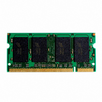
MT4VDDT3264HY-335F2 Micron Technology Inc, MT4VDDT3264HY-335F2 Datasheet - Page 22

MT4VDDT3264HY-335F2
Manufacturer Part Number
MT4VDDT3264HY-335F2
Description
MODULE DDR 256MB 200-SODIMM
Manufacturer
Micron Technology Inc
Specifications of MT4VDDT3264HY-335F2
Memory Type
DDR SDRAM
Memory Size
256MB
Speed
333MT/s
Package / Case
200-SODIMM
Main Category
DRAM Module
Sub-category
DDR SDRAM
Module Type
200SODIMM
Device Core Size
64b
Organization
32Mx64
Total Density
256MByte
Chip Density
512Mb
Access Time (max)
700ps
Maximum Clock Rate
333MHz
Operating Supply Voltage (typ)
2.5V
Operating Current
780mA
Number Of Elements
4
Operating Supply Voltage (max)
2.7V
Operating Supply Voltage (min)
2.3V
Operating Temp Range
0C to 70C
Operating Temperature Classification
Commercial
Pin Count
200
Mounting
Socket
Lead Free Status / RoHS Status
Lead free / RoHS Compliant
Other names
557-1231
MT4VDDT3264HY-335F2
MT4VDDT3264HY-335F2
SDA
SPD Clock and Data Conventions
SCL LOW. SDA state changes during SCL HIGH are
reserved for indicating start and stop conditions (as
shown in Figure 12, Data Validity, and Figure 13, Defi-
nition of Start and Stop).
SPD Start Condition
which is a HIGH-to-LOW transition of SDA when SCL
is HIGH. The SPD device continuously monitors the
SDA and SCL lines for the start condition and will not
respond to any command until this condition has been
met.
SPD Stop Condition
tion, which is a LOW-to-HIGH transition of SDA when
SCL is HIGH. The stop condition is also used to place
the SPD device into standby power mode.
pdf: 09005aef80b56d1b, source: 09005aef8086ea0b
DDA4C16_32x64HG.fm - Rev. D 9/04 EN
SCL from Master
Data Output
from Transmitter
Data Output
from Receiver
SCL
Data states on the SDA line can change only during
All commands are preceded by the start condition,
All communications are terminated by a stop condi-
Figure 12: Data Validity
DATA STABLE
Figure 14: Acknowledge Response from Receiver
DATA
CHANGE
DATA STABLE
22
SDA
SPD Acknowledge
cate successful data transfers. The transmitting device,
either master or slave, will release the bus after trans-
mitting eight bits. During the ninth clock cycle, the
receiver will pull the SDA line LOW to acknowledge
that it received the eight bits of data (as shown in Fig-
ure 14, Acknowledge Response from Receiver).
acknowledge after recognition of a start condition and
its slave address. If both the device and a WRITE oper-
ation have been selected, the SPD device will respond
with an acknowledge after the receipt of each subse-
quent eight-bit word. In the read mode the SPD device
will transmit eight bits of data, release the SDA line and
monitor the line for an acknowledge. If an acknowl-
edge is detected and no stop condition is generated by
the master, the slave will continue to transmit data. If
an acknowledge is not detected, the slave will termi-
nate further data transmissions and await the stop
condition to return to standby power mode.
Figure 13: Definition of Start and Stop
SCL
128MB, 256MB (x64, SR) PC3200
Acknowledge is a software convention used to indi-
The SPD device will always respond with an
200-PIN DDR SDRAM SODIMM
Micron Technology, Inc., reserves the right to change products or specifications without notice.
START
BIT
8
Acknowledge
©2004 Micron Technology, Inc.
9
STOP
BIT


