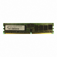
MT9VDDF6472Y-335F1 Micron Technology Inc, MT9VDDF6472Y-335F1 Datasheet - Page 11

MT9VDDF6472Y-335F1
Manufacturer Part Number
MT9VDDF6472Y-335F1
Description
MODULE DDR SDRAM 512MB 184-DIMM
Manufacturer
Micron Technology Inc
Specifications of MT9VDDF6472Y-335F1
Memory Type
DDR SDRAM
Memory Size
512MB
Speed
167MHz
Package / Case
184-DIMM
Main Category
DRAM Module
Sub-category
DDR SDRAM
Module Type
184RDIMM
Device Core Size
72b
Organization
64Mx72
Total Density
512MByte
Chip Density
512Mb
Maximum Clock Rate
333MHz
Operating Supply Voltage (typ)
2.5V
Operating Current
1.575A
Number Of Elements
9
Operating Supply Voltage (max)
2.7V
Operating Supply Voltage (min)
2.3V
Operating Temp Range
0C to 70C
Operating Temperature Classification
Commercial
Pin Count
184
Mounting
Socket
Lead Free Status / RoHS Status
Lead free / RoHS Compliant
Other names
557-1293
MT9VDDF6472Y-335F1
MT9VDDF6472Y-335F1
Table 6:
NOTE:
Table 7:
pdf: 09005aef80e119b2, source: 09005aef807d56a1
DDF9C32_64x72G.fm - Rev. B 9/04 EN
LENGTH
1. For a burst length of two, A1–Ai select the two-data-
2. For a burst length of four, A2–Ai select the four-data-
3. For a burst length of eight, A3–Ai select the eight-data-
4. Whenever a boundary of the block is reached within a
5. i = 9 for 256MB,
BURST
element block; A0 selects the first access within the
block.
element block; A0–A1 select the first access within the
block.
element block; A0–A2 select the first access within the
block.
given sequence above, the following access wraps
within the block.
i = 9, 11 for 512MB
2
4
8
SPEED
-26A
-335
-262
-265
-202
A2 A1 A0
0
0
0
0
1
1
1
1
STARTING
ADDRESS
COLUMN
Burst Definition Table
CAS Latency Table
A1 A0
0
0
1
1
0
0
1
1
0
0
1
1
A0
75
75
75
75
75
0
1
0
1
0
1
0
1
0
1
0
1
0
1
CLOCK FREQUENCY (MHZ)
CL = 2
ALLOWABLE OPERATING
f
f
f
f
f
ORDER OF ACCESSES WITHIN
0-1-2-3-4-5-6-7 0-1-2-3-4-5-6-7
1-2-3-4-5-6-7-0 1-0-3-2-5-4-7-6
2-3-4-5-6-7-0-1 2-3-0-1-6-7-4-5
3-4-5-6-7-0-1-2 3-2-1-0-7-6-5-4
4-5-6-7-0-1-2-3 4-5-6-7-0-1-2-3
5-6-7-0-1-2-3-4 5-4-7-6-1-0-3-2
6-7-0-1-2-3-4-5 6-7-4-5-2-3-0-1
7-0-1-2-3-4-5-6 7-6-5-4-3-2-1-0
SEQUENTIAL
133
133
133
100
100
TYPE =
0-1-2-3
1-2-3-0
2-3-0-1
3-0-1-2
0-1
1-0
A BURST
75
75
75
75
75
INTERLEAVED
CL = 2.5
TYPE =
0-1-2-3
1-0-3-2
2-3-0-1
3-2-1-0
f
f
f
f
f
0-1
1-0
167
133
133
133
125
11
Operating Mode
MODE REGISTER SET command with bits A7–A12
each set to zero, and bits A0–A6 set to the desired val-
ues. A DLL reset is initiated by issuing a MODE REGIS-
TER SET command with bits A7 and A9–A12 each set
to zero, bit A8 set to one, and bits A0–A6 set to the
desired values. Although not required by the Micron
device, JEDEC specifications recommend when a
LOAD MODE REGISTER command is issued to reset
the DLL, it should always be followed by a LOAD
MODE REGISTER command to select normal operat-
ing mode.
reserved for future use and/or test modes. Test modes
and reserved states should not be used because
unknown operation or incompatibility with future ver-
sions may result.
Extended Mode Register
beyond those controlled by the mode register; these
additional functions are DLL enable/disable and out-
put drive strength. These functions are controlled via
the bits shown in Figure 8, Extended Mode Register
Definition Diagram. The extended mode register is
programmed via the LOAD MODE REGISTER com-
mand to the mode register (with BA0 = 1 and BA1 = 0)
COMMAND
COMMAND
The normal operating mode is selected by issuing a
All other combinations of values for A7–A12 are
The extended mode register controls functions
DQS
DQS
CK#
CK#
DQ
DQ
256MB, 512MB (x72, ECC, SR)
Micron Technology, Inc., reserves the right to change products or specifications without notice.
Figure 7: CAS Latency Diagram
CK
CK
184-PIN DDR SDRAM RDIMM
READ
READ
Burst Length = 4 in the cases shown
Shown with nominal t AC, t DQSCK, and t DQSQ
T0
T0
CL = 2
TRANSITIONING DATA
CL = 2.5
NOP
NOP
T1
T1
©2004 Micron Technology, Inc. All rights reserved.
T2
NOP
NOP
T2
T2n
T2n
DON’T CARE
T3
NOP
NOP
T3
T3n
T3n


