MT36HTJ51272Y-40EA2 Micron Technology Inc, MT36HTJ51272Y-40EA2 Datasheet
MT36HTJ51272Y-40EA2
Specifications of MT36HTJ51272Y-40EA2


Related parts for MT36HTJ51272Y-40EA2


MT36HTJ51272Y-40EA2 Summary of contents
Page 1
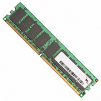
DDR2 SDRAM Registered DIMM (RDIMM) MT36HTJ51272(P) – 4GB For the latest data sheet and for component data sheets, refer to Micron's Web site: Features • Supports 95 C with double refresh ° • 240-pin, registered dual in-line memory module • ...
Page 2
... MT36HTJ51272(P)Y-667__ MT36HTJ51272(P)Y-53E__ MT36HTJ51272(P)Y-40E__ Notes: 1. All part numbers end with a two-place code (not shown), designating component and PCB revisions. Consult factory for current revision codes. Example: MT36HTJ51272Y-667C2. Pin Assignments and Descriptions Table 4: Pin Assignments 240-Pin RDIMM Front Pin Symbol Pin Symbol Pin Symbol Pin Symbol ...
Page 3
Table 5: Pin Descriptions Symbol Type ODT0, ODT1 Input On-die termination: ODT (registered HIGH) enables termination resistance internal to the (SSTL18) DDR2 SDRAM. When enabled, ODT is only applied to the following pins: DQ, DQS, DQS#, and CB. The ODT ...
Page 4
Functional Block Diagram Figure 2: Functional Block Diagram Rank 0 = U1b-U5b, U9b-U16b, U18b-U22b Rank 1 = U1t-U5t, U9t-U16t, U18t-U22t U7 Serial PD SCL SDA SA0 SA1 SA2 U6, U17 ...
Page 5
... READs and by the memory controller during WRITEs. DQS is edge- aligned with data for READs and center-aligned with data for WRITEs. DDR2 SDRAM modules operate from a differential clock (CK and CK#); the crossing of CK going HIGH and CK# going LOW will be referred to as the positive edge of CK. ...
Page 6
... When inductance and delay parameters associated with trace lengths are used in simulations, they are significantly more accurate and real- istic than a gross estimation of module capacitance. Simulations can then render a considerably more accurate result. JEDEC modules are now designed by using simula- tions to close timing budgets. I ...
Page 7
Table 7: DDR2 I Specifications and Conditions – 4GB (continued) DD Values shown for MT47H256M4 DDR2 SDRAM only and are computed from values specified in the 1Gb (256 Meg x 4) component data sheet Parameter/Condition Precharge power-down current: All device ...
Page 8
AC Timing and Operating Conditions Recommended AC operating conditions are given in the DDR2 component data sheets. Component specifications are available on Micron’s Web site: www.micron.com. Module speed grades correlate with component speed grades as shown in Table 8: Table ...
Page 9
PLL Table 10: PLL (CU877 device or equivalent JESD82-8.01) Parameter Symbol V DC high-level input voltage DC low-level input voltage V Input voltage (limits high-level input voltage low-level input voltage Input differential-pair cross V voltage ...
Page 10
Table 11: PLL Clock Driver Timing Requirements and Switching Characteristics Note: 1 Parameter Stabilization time Input clock slew rate SSC modulation frequency SSC clock input frequency deviation PLL loop bandwidth (–3dB from unity gain) Notes: 1. PLL specifications are critical ...
Page 11
Table 13: Serial Presence-Detect EEPROM AC Operating Conditions All voltages referenced to V Parameter/Condition SCL LOW to SDA data-out valid Time the bus must be free before a new transition can start Data-out hold time SDA and SCL fall time ...
Page 12
Table 14: Serial Presence-Detect Matrix “1”/“0”: serial data, “driven to HIGH”/“driven to LOW” Byte 0 Number of SPD bytes used by Micron 1 Total number of bytes in SPD device 2 Fundamental memory type 3 Number of row addresses on ...
Page 13
Table 14: Serial Presence-Detect Matrix (continued) “1”/“0”: serial data, “driven to HIGH”/“driven to LOW” Byte 32 Address and command setup time, 33 Address and command hold time, 34 Data/data mask input setup time, 35 Data/data mask input hold time, t ...
Page 14
Module Dimensions Figure 3: 240-Pin DDR2 DIMM 2.00 (0.079) R (4X 2.50 (0.098) D (2X) 2.30 (0.091) TYP PIN 1 2.21 (0.087) TYP 1.0 (0.039) TYP 70.66 (2.782) TYP U13 U14 U15 PIN 240 3.04 (0.1197) TYP ...