C8051T610DB32 Silicon Laboratories Inc, C8051T610DB32 Datasheet - Page 164
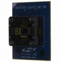
C8051T610DB32
Manufacturer Part Number
C8051T610DB32
Description
DAUGHT BOARD T610 32TQFP SOCKET
Manufacturer
Silicon Laboratories Inc
Datasheet
1.C8051T610DB32.pdf
(218 pages)
Specifications of C8051T610DB32
Module/board Type
Socket Module - TQFP
Processor To Be Evaluated
C8051T61x
Interface Type
USB
Lead Free Status / RoHS Status
Lead free / RoHS Compliant
For Use With/related Products
C8051T610DK
Lead Free Status / RoHS Status
Lead free / RoHS Compliant, Lead free / RoHS Compliant
Other names
336-1505


C8051T610/1/2/3/4/5/6/7
SFR Definition 24.1. SPI0CFG: SPI0 Configuration
SFR Address = 0xA1
164
Note: In slave mode, data on MOSI is sampled in the center of each data bit. In master mode, data on MISO is
Name
Reset
Bit
Type
7
6
5
4
3
2
1
0
Bit
sampled one SYSCLK before the end of each data bit, to provide maximum settling time for the slave device.
See Table 24.1 for timing parameters.
SLVSEL
SPIBSY
MSTEN
RXBMT
CKPHA
CKPOL
SPIBSY
NSSIN
SRMT
Name
R
7
0
MSTEN
SPI Busy.
This bit is set to logic 1 when a SPI transfer is in progress (master or slave mode).
Master Mode Enable.
0: Disable master mode. Operate in slave mode.
1: Enable master mode. Operate as a master.
SPI0 Clock Phase.
0: Data centered on first edge of SCK period.
1: Data centered on second edge of SCK period.
SPI0 Clock Polarity.
0: SCK line low in idle state.
1: SCK line high in idle state.
Slave Selected Flag.
This bit is set to logic 1 whenever the NSS pin is low indicating SPI0 is the selected
slave. It is cleared to logic 0 when NSS is high (slave not selected). This bit does
not indicate the instantaneous value at the NSS pin, but rather a de-glitched ver-
sion of the pin input.
NSS Instantaneous Pin Input.
This bit mimics the instantaneous value that is present on the NSS port pin at the
time that the register is read. This input is not de-glitched.
Shift Register Empty (valid in slave mode only).
This bit will be set to logic 1 when all data has been transferred in/out of the shift
register, and there is no new information available to read from the transmit buffer
or write to the receive buffer. It returns to logic 0 when a data byte is transferred to
the shift register from the transmit buffer or by a transition on SCK. SRMT = 1 when
in Master Mode.
Receive Buffer Empty (valid in slave mode only).
This bit will be set to logic 1 when the receive buffer has been read and contains no
new information. If there is new information available in the receive buffer that has
not been read, this bit will return to logic 0. RXBMT = 1 when in Master Mode.
R/W
6
0
CKPHA
R/W
5
0
CKPOL
R/W
Rev 1.0
4
0
SLVSEL
Function
R
3
0
*
NSSIN
*
R
2
1
SRMT
R
1
1
RXBMT
R
0
1
Related parts for C8051T610DB32
Image
Part Number
Description
Manufacturer
Datasheet
Request
R

Part Number:
Description:
SMD/C°/SINGLE-ENDED OUTPUT SILICON OSCILLATOR
Manufacturer:
Silicon Laboratories Inc
Part Number:
Description:
Manufacturer:
Silicon Laboratories Inc
Datasheet:
Part Number:
Description:
N/A N/A/SI4010 AES KEYFOB DEMO WITH LCD RX
Manufacturer:
Silicon Laboratories Inc
Datasheet:
Part Number:
Description:
N/A N/A/SI4010 SIMPLIFIED KEY FOB DEMO WITH LED RX
Manufacturer:
Silicon Laboratories Inc
Datasheet:
Part Number:
Description:
N/A/-40 TO 85 OC/EZLINK MODULE; F930/4432 HIGH BAND (REV E/B1)
Manufacturer:
Silicon Laboratories Inc
Part Number:
Description:
EZLink Module; F930/4432 Low Band (rev e/B1)
Manufacturer:
Silicon Laboratories Inc
Part Number:
Description:
I°/4460 10 DBM RADIO TEST CARD 434 MHZ
Manufacturer:
Silicon Laboratories Inc
Part Number:
Description:
I°/4461 14 DBM RADIO TEST CARD 868 MHZ
Manufacturer:
Silicon Laboratories Inc
Part Number:
Description:
I°/4463 20 DBM RFSWITCH RADIO TEST CARD 460 MHZ
Manufacturer:
Silicon Laboratories Inc
Part Number:
Description:
I°/4463 20 DBM RADIO TEST CARD 868 MHZ
Manufacturer:
Silicon Laboratories Inc
Part Number:
Description:
I°/4463 27 DBM RADIO TEST CARD 868 MHZ
Manufacturer:
Silicon Laboratories Inc
Part Number:
Description:
I°/4463 SKYWORKS 30 DBM RADIO TEST CARD 915 MHZ
Manufacturer:
Silicon Laboratories Inc
Part Number:
Description:
N/A N/A/-40 TO 85 OC/4463 RFMD 30 DBM RADIO TEST CARD 915 MHZ
Manufacturer:
Silicon Laboratories Inc
Part Number:
Description:
I°/4463 20 DBM RADIO TEST CARD 169 MHZ
Manufacturer:
Silicon Laboratories Inc