C8051T610DB32 Silicon Laboratories Inc, C8051T610DB32 Datasheet - Page 8
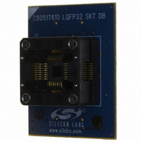
C8051T610DB32
Manufacturer Part Number
C8051T610DB32
Description
DAUGHT BOARD T610 32TQFP SOCKET
Manufacturer
Silicon Laboratories Inc
Datasheet
1.C8051T610DB32.pdf
(218 pages)
Specifications of C8051T610DB32
Module/board Type
Socket Module - TQFP
Processor To Be Evaluated
C8051T61x
Interface Type
USB
Lead Free Status / RoHS Status
Lead free / RoHS Compliant
For Use With/related Products
C8051T610DK
Lead Free Status / RoHS Status
Lead free / RoHS Compliant, Lead free / RoHS Compliant
Other names
336-1505


C8051T610/1/2/3/4/5/6/7
19. Reset Sources
20. Oscillators and Clock Selection
21. Port Input/Output
22. SMBus
23. UART0
24. Enhanced Serial Peripheral Interface (SPI0)
25. Timers
8
Figure 19.1. Reset Sources ................................................................................... 100
Figure 19.2. Power-On and VDD Monitor Reset Timing ....................................... 101
Figure 20.1. Oscillator Options .............................................................................. 106
Figure 21.1. Port I/O Functional Block Diagram .................................................... 113
Figure 21.2. Port I/O Cell Block Diagram .............................................................. 115
Figure 21.3. Priority Crossbar Decoder Potential Pin Assignments ...................... 118
Figure 21.4. Priority Crossbar Decoder Example 1 - No Skipped Pins ................. 119
Figure 21.5. Priority Crossbar Decoder Example 2 - Skipping Pins ...................... 120
Figure 22.1. SMBus Block Diagram ...................................................................... 132
Figure 22.2. Typical SMBus Configuration ............................................................ 133
Figure 22.3. SMBus Transaction ........................................................................... 134
Figure 22.4. Typical SMBus SCL Generation ........................................................ 136
Figure 22.5. Typical Master Write Sequence ........................................................ 143
Figure 22.6. Typical Master Read Sequence ........................................................ 144
Figure 22.7. Typical Slave Write Sequence .......................................................... 145
Figure 22.8. Typical Slave Read Sequence .......................................................... 146
Figure 23.1. UART0 Block Diagram ...................................................................... 149
Figure 23.2. UART0 Baud Rate Logic ................................................................... 150
Figure 23.3. UART Interconnect Diagram ............................................................. 151
Figure 23.4. 8-Bit UART Timing Diagram .............................................................. 151
Figure 23.5. 9-Bit UART Timing Diagram .............................................................. 152
Figure 23.6. UART Multi-Processor Mode Interconnect Diagram ......................... 153
Figure 24.1. SPI Block Diagram ............................................................................ 157
Figure 24.2. Multiple-Master Mode Connection Diagram ...................................... 159
Figure 24.3. 3-Wire Single Master and 3-Wire Single Slave Mode
Figure 24.4. 4-Wire Single Master Mode and 4-Wire Slave Mode
Figure 24.5. Master Mode Data/Clock Timing ....................................................... 162
Figure 24.6. Slave Mode Data/Clock Timing (CKPHA = 0) ................................... 162
Figure 24.7. Slave Mode Data/Clock Timing (CKPHA = 1) ................................... 163
Figure 24.8. SPI Master Timing (CKPHA = 0) ....................................................... 167
Figure 24.9. SPI Master Timing (CKPHA = 1) ....................................................... 167
Figure 24.10. SPI Slave Timing (CKPHA = 0) ....................................................... 168
Figure 24.11. SPI Slave Timing (CKPHA = 1) ....................................................... 168
Figure 25.1. T0 Mode 0 Block Diagram ................................................................. 173
Figure 25.2. T0 Mode 2 Block Diagram ................................................................. 174
Figure 25.3. T0 Mode 3 Block Diagram ................................................................. 175
Connection Diagram ........................................................................................ 160
Connection Diagram ........................................................................................ 160
Rev 1.0
Related parts for C8051T610DB32
Image
Part Number
Description
Manufacturer
Datasheet
Request
R

Part Number:
Description:
SMD/C°/SINGLE-ENDED OUTPUT SILICON OSCILLATOR
Manufacturer:
Silicon Laboratories Inc
Part Number:
Description:
Manufacturer:
Silicon Laboratories Inc
Datasheet:
Part Number:
Description:
N/A N/A/SI4010 AES KEYFOB DEMO WITH LCD RX
Manufacturer:
Silicon Laboratories Inc
Datasheet:
Part Number:
Description:
N/A N/A/SI4010 SIMPLIFIED KEY FOB DEMO WITH LED RX
Manufacturer:
Silicon Laboratories Inc
Datasheet:
Part Number:
Description:
N/A/-40 TO 85 OC/EZLINK MODULE; F930/4432 HIGH BAND (REV E/B1)
Manufacturer:
Silicon Laboratories Inc
Part Number:
Description:
EZLink Module; F930/4432 Low Band (rev e/B1)
Manufacturer:
Silicon Laboratories Inc
Part Number:
Description:
I°/4460 10 DBM RADIO TEST CARD 434 MHZ
Manufacturer:
Silicon Laboratories Inc
Part Number:
Description:
I°/4461 14 DBM RADIO TEST CARD 868 MHZ
Manufacturer:
Silicon Laboratories Inc
Part Number:
Description:
I°/4463 20 DBM RFSWITCH RADIO TEST CARD 460 MHZ
Manufacturer:
Silicon Laboratories Inc
Part Number:
Description:
I°/4463 20 DBM RADIO TEST CARD 868 MHZ
Manufacturer:
Silicon Laboratories Inc
Part Number:
Description:
I°/4463 27 DBM RADIO TEST CARD 868 MHZ
Manufacturer:
Silicon Laboratories Inc
Part Number:
Description:
I°/4463 SKYWORKS 30 DBM RADIO TEST CARD 915 MHZ
Manufacturer:
Silicon Laboratories Inc
Part Number:
Description:
N/A N/A/-40 TO 85 OC/4463 RFMD 30 DBM RADIO TEST CARD 915 MHZ
Manufacturer:
Silicon Laboratories Inc
Part Number:
Description:
I°/4463 20 DBM RADIO TEST CARD 169 MHZ
Manufacturer:
Silicon Laboratories Inc