C8051T610DB24 Silicon Laboratories Inc, C8051T610DB24 Datasheet - Page 120
C8051T610DB24
Manufacturer Part Number
C8051T610DB24
Description
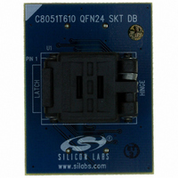
DAUGHTER BOARD T610 24QFN SOCKET
Manufacturer
Silicon Laboratories Inc
Datasheet
1.C8051T610DB32.pdf
(218 pages)
Specifications of C8051T610DB24
Module/board Type
Socket Module - QFN
Processor To Be Evaluated
C8051T61x
Interface Type
USB
Lead Free Status / RoHS Status
Lead free / RoHS Compliant
For Use With/related Products
C8051T610DK
Lead Free Status / RoHS Status
Lead free / RoHS Compliant, Lead free / RoHS Compliant
Other names
336-1507


C8051T610/1/2/3/4/5/6/7
120
In this example, the crossbar is configured to assign the UART TX0 and RX0 signals, the
SMBus signals, and the SYSCLK signal. Note that the SMBus signals are assigned as a
pair. Additionally, pins P0.0 and P0.3 are configured to be skipped using the XBR0 register.
configuration.
1
2
3
4
All unassigned pins, including those skipped by XBR0 can be used as GPIO or for other non-
crossbar functions.
Pin Number
st
nd
rd
th
TX0 is assigned to P0.4
SYSCLK
SDA and SCL are assigned to P0.2 and P0.3, respectively.
SYSCLK is assigned to P0.6
Function
Figure 21.5. Priority Crossbar Decoder Example 2 - Skipping Pins
RX0 is assigned to P0.5
Pin Skip
These boxes represent the port pins which are used by the peripherals in this
Settings
Special
Signals
CP0A
CP1A
CEX0
CEX1
CEX2
CEX3
CEX4
MISO
MOSI
NSS*
SCK
SDA
RX0
SCL
CP0
CP1
Port
TX0
ECI
T0
T1
0 1 2 3 4 5 6 7
1 0 0 1 0 0 0 0
P0SKIP
P0
0 1 2 3 4 5 6 7
0 0 0 0 0 0 0 0
Rev 1.0
P1SKIP
P1
0 1 2 3 4 5 6 7
0 0 0 0 x x x x
P2SKIP
P2
Related parts for C8051T610DB24
Image
Part Number
Description
Manufacturer
Datasheet
Request
R

Part Number:
Description:
SMD/C°/SINGLE-ENDED OUTPUT SILICON OSCILLATOR
Manufacturer:
Silicon Laboratories Inc
Part Number:
Description:
Manufacturer:
Silicon Laboratories Inc
Datasheet:
Part Number:
Description:
N/A N/A/SI4010 AES KEYFOB DEMO WITH LCD RX
Manufacturer:
Silicon Laboratories Inc
Datasheet:
Part Number:
Description:
N/A N/A/SI4010 SIMPLIFIED KEY FOB DEMO WITH LED RX
Manufacturer:
Silicon Laboratories Inc
Datasheet:
Part Number:
Description:
N/A/-40 TO 85 OC/EZLINK MODULE; F930/4432 HIGH BAND (REV E/B1)
Manufacturer:
Silicon Laboratories Inc
Part Number:
Description:
EZLink Module; F930/4432 Low Band (rev e/B1)
Manufacturer:
Silicon Laboratories Inc
Part Number:
Description:
I°/4460 10 DBM RADIO TEST CARD 434 MHZ
Manufacturer:
Silicon Laboratories Inc
Part Number:
Description:
I°/4461 14 DBM RADIO TEST CARD 868 MHZ
Manufacturer:
Silicon Laboratories Inc
Part Number:
Description:
I°/4463 20 DBM RFSWITCH RADIO TEST CARD 460 MHZ
Manufacturer:
Silicon Laboratories Inc
Part Number:
Description:
I°/4463 20 DBM RADIO TEST CARD 868 MHZ
Manufacturer:
Silicon Laboratories Inc
Part Number:
Description:
I°/4463 27 DBM RADIO TEST CARD 868 MHZ
Manufacturer:
Silicon Laboratories Inc
Part Number:
Description:
I°/4463 SKYWORKS 30 DBM RADIO TEST CARD 915 MHZ
Manufacturer:
Silicon Laboratories Inc
Part Number:
Description:
N/A N/A/-40 TO 85 OC/4463 RFMD 30 DBM RADIO TEST CARD 915 MHZ
Manufacturer:
Silicon Laboratories Inc
Part Number:
Description:
I°/4463 20 DBM RADIO TEST CARD 169 MHZ
Manufacturer:
Silicon Laboratories Inc