C8051T610DB24 Silicon Laboratories Inc, C8051T610DB24 Datasheet - Page 124
C8051T610DB24
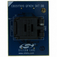
Manufacturer Part Number
C8051T610DB24
Description
DAUGHTER BOARD T610 24QFN SOCKET
Manufacturer
Silicon Laboratories Inc
Datasheet
1.C8051T610DB32.pdf
(218 pages)
Specifications of C8051T610DB24
Module/board Type
Socket Module - QFN
Processor To Be Evaluated
C8051T61x
Interface Type
USB
Lead Free Status / RoHS Status
Lead free / RoHS Compliant
For Use With/related Products
C8051T610DK
Lead Free Status / RoHS Status
Lead free / RoHS Compliant, Lead free / RoHS Compliant
Other names
336-1507


C8051T610/1/2/3/4/5/6/7
21.5. Special Function Registers for Accessing and Configuring Port I/O
All Port I/O are accessed through corresponding special function registers (SFRs) that are both byte
addressable and bit addressable. When writing to a Port, the value written to the SFR is latched to main-
tain the output data value at each pin. When reading, the logic levels of the Port's input pins are returned
regardless of the XBRn settings (i.e., even when the pin is assigned to another signal by the Crossbar, the
Port register can always read its corresponding Port I/O pin). The exception to this is the execution of the
read-modify-write instructions that target a Port Latch register as the destination. The read-modify-write
instructions when operating on a Port SFR are the following: ANL, ORL, XRL, JBC, CPL, INC, DEC, DJNZ
and MOV, CLR or SETB, when the destination is an individual bit in a Port SFR. For these instructions, the
value of the latch register (not the pin) is read, modified, and written back to the SFR.
Each Port has a corresponding PnSKIP register which allows its individual Port pins to be assigned to dig-
ital functions or skipped by the Crossbar. All Port pins used for analog functions, GPIO, or dedicated digital
functions such as the EMIF should have their PnSKIP bit set to 1.
The Port input mode of the I/O pins is defined using the Port Input Mode registers (PnMDIN). Each Port
cell can be configured for analog or digital I/O. This selection is required even for the digital resources
selected in the XBRn registers, and is not automatic.
The output driver characteristics of the I/O pins are defined using the Port Output Mode registers (PnMD-
OUT). Each Port Output driver can be configured as either open drain or push-pull. This selection is
required even for the digital resources selected in the XBRn registers, and is not automatic. The only
exception to this is the SMBus (SDA, SCL) pins, which are configured as open-drain regardless of the
PnMDOUT settings.
SFR Definition 21.3. P0: Port 0
SFR Address = 0x80; Bit-Addressable
124
Name
Reset
7:0
Bit
Type
Bit
P0[7:0]
Name
7
1
Port 0 Data.
Sets the Port latch logic
value or reads the Port pin
logic state in Port cells con-
figured for digital I/O.
6
1
Description
5
1
0: Set output latch to logic
LOW.
1: Set output latch to logic
HIGH.
Rev 1.0
4
1
P0[7:0]
R/W
Write
3
1
2
1
0: P0.n Port pin is logic
LOW.
1: P0.n Port pin is logic
HIGH.
1
1
Read
0
1
Related parts for C8051T610DB24
Image
Part Number
Description
Manufacturer
Datasheet
Request
R

Part Number:
Description:
SMD/C°/SINGLE-ENDED OUTPUT SILICON OSCILLATOR
Manufacturer:
Silicon Laboratories Inc
Part Number:
Description:
Manufacturer:
Silicon Laboratories Inc
Datasheet:
Part Number:
Description:
N/A N/A/SI4010 AES KEYFOB DEMO WITH LCD RX
Manufacturer:
Silicon Laboratories Inc
Datasheet:
Part Number:
Description:
N/A N/A/SI4010 SIMPLIFIED KEY FOB DEMO WITH LED RX
Manufacturer:
Silicon Laboratories Inc
Datasheet:
Part Number:
Description:
N/A/-40 TO 85 OC/EZLINK MODULE; F930/4432 HIGH BAND (REV E/B1)
Manufacturer:
Silicon Laboratories Inc
Part Number:
Description:
EZLink Module; F930/4432 Low Band (rev e/B1)
Manufacturer:
Silicon Laboratories Inc
Part Number:
Description:
I°/4460 10 DBM RADIO TEST CARD 434 MHZ
Manufacturer:
Silicon Laboratories Inc
Part Number:
Description:
I°/4461 14 DBM RADIO TEST CARD 868 MHZ
Manufacturer:
Silicon Laboratories Inc
Part Number:
Description:
I°/4463 20 DBM RFSWITCH RADIO TEST CARD 460 MHZ
Manufacturer:
Silicon Laboratories Inc
Part Number:
Description:
I°/4463 20 DBM RADIO TEST CARD 868 MHZ
Manufacturer:
Silicon Laboratories Inc
Part Number:
Description:
I°/4463 27 DBM RADIO TEST CARD 868 MHZ
Manufacturer:
Silicon Laboratories Inc
Part Number:
Description:
I°/4463 SKYWORKS 30 DBM RADIO TEST CARD 915 MHZ
Manufacturer:
Silicon Laboratories Inc
Part Number:
Description:
N/A N/A/-40 TO 85 OC/4463 RFMD 30 DBM RADIO TEST CARD 915 MHZ
Manufacturer:
Silicon Laboratories Inc
Part Number:
Description:
I°/4463 20 DBM RADIO TEST CARD 169 MHZ
Manufacturer:
Silicon Laboratories Inc