C8051T610DB24 Silicon Laboratories Inc, C8051T610DB24 Datasheet - Page 45
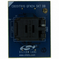
C8051T610DB24
Manufacturer Part Number
C8051T610DB24
Description
DAUGHTER BOARD T610 24QFN SOCKET
Manufacturer
Silicon Laboratories Inc
Datasheet
1.C8051T610DB32.pdf
(218 pages)
Specifications of C8051T610DB24
Module/board Type
Socket Module - QFN
Processor To Be Evaluated
C8051T61x
Interface Type
USB
Lead Free Status / RoHS Status
Lead free / RoHS Compliant
For Use With/related Products
C8051T610DK
Lead Free Status / RoHS Status
Lead free / RoHS Compliant, Lead free / RoHS Compliant
Other names
336-1507


SFR Definition 8.4. ADC0CN: ADC0 Control
SFR Address = 0xE8; Bit-Addressable
Name
Reset
Bit
2:0 AD0CM[2:0] ADC0 Start of Conversion Mode Select.
Type
7
6
5
4
3
Bit
AD0BUSY ADC0 Busy Bit.
AD0WINT
AD0INT
AD0EN
AD0TM
Name
AD0EN
R/W
7
0
ADC0 Enable Bit.
0: ADC0 Disabled. ADC0 is in low-power shutdown.
1: ADC0 Enabled. ADC0 is active and ready for data conversions.
ADC0 Track Mode Bit.
0: Normal Track Mode: When ADC0 is enabled, tracking is continuous unless a con-
version is in progress. Conversion begins immediately on start-of-conversion event,
as defined by AD0CM[2:0].
1: Delayed Track Mode: When ADC0 is enabled, input is tracked when a conversion
is not in progress. A start-of-conversion signal initiates three SAR clocks of additional
tracking, and then begins the conversion.
ADC0 Conversion Complete Interrupt Flag.
0: ADC0 has not completed a data conversion since AD0INT was last cleared.
1: ADC0 has completed a data conversion.
ADC0 Window Compare Interrupt Flag.
0: ADC0 Window Comparison Data match has not occurred since this flag was last
cleared.
1: ADC0 Window Comparison Data match has occurred.
000: ADC0 start-of-conversion source is write of 1 to AD0BUSY.
001: ADC0 start-of-conversion source is overflow of Timer 0.
010: ADC0 start-of-conversion source is overflow of Timer 2.
011: ADC0 start-of-conversion source is overflow of Timer 1.
100: ADC0 start-of-conversion source is rising edge of external CNVSTR.
101: ADC0 start-of-conversion source is overflow of Timer 3.
11x: Reserved.
AD0TM
R/W
6
0
AD0INT
R/W
5
0
Read:
0: ADC0 conversion is not in
progress.
1: ADC0 conversion is in prog-
ress.
AD0BUSY AD0WINT
R/W
Rev 1.0
4
0
C8051T610/1/2/3/4/5/6/7
Function
R/W
3
0
Write:
0: No Effect.
1: Initiates ADC0 Conversion if
AD0CM[2:0] = 000b
2
0
AD0CM[2:0]
R/W
1
0
0
0
45
Related parts for C8051T610DB24
Image
Part Number
Description
Manufacturer
Datasheet
Request
R

Part Number:
Description:
SMD/C°/SINGLE-ENDED OUTPUT SILICON OSCILLATOR
Manufacturer:
Silicon Laboratories Inc
Part Number:
Description:
Manufacturer:
Silicon Laboratories Inc
Datasheet:
Part Number:
Description:
N/A N/A/SI4010 AES KEYFOB DEMO WITH LCD RX
Manufacturer:
Silicon Laboratories Inc
Datasheet:
Part Number:
Description:
N/A N/A/SI4010 SIMPLIFIED KEY FOB DEMO WITH LED RX
Manufacturer:
Silicon Laboratories Inc
Datasheet:
Part Number:
Description:
N/A/-40 TO 85 OC/EZLINK MODULE; F930/4432 HIGH BAND (REV E/B1)
Manufacturer:
Silicon Laboratories Inc
Part Number:
Description:
EZLink Module; F930/4432 Low Band (rev e/B1)
Manufacturer:
Silicon Laboratories Inc
Part Number:
Description:
I°/4460 10 DBM RADIO TEST CARD 434 MHZ
Manufacturer:
Silicon Laboratories Inc
Part Number:
Description:
I°/4461 14 DBM RADIO TEST CARD 868 MHZ
Manufacturer:
Silicon Laboratories Inc
Part Number:
Description:
I°/4463 20 DBM RFSWITCH RADIO TEST CARD 460 MHZ
Manufacturer:
Silicon Laboratories Inc
Part Number:
Description:
I°/4463 20 DBM RADIO TEST CARD 868 MHZ
Manufacturer:
Silicon Laboratories Inc
Part Number:
Description:
I°/4463 27 DBM RADIO TEST CARD 868 MHZ
Manufacturer:
Silicon Laboratories Inc
Part Number:
Description:
I°/4463 SKYWORKS 30 DBM RADIO TEST CARD 915 MHZ
Manufacturer:
Silicon Laboratories Inc
Part Number:
Description:
N/A N/A/-40 TO 85 OC/4463 RFMD 30 DBM RADIO TEST CARD 915 MHZ
Manufacturer:
Silicon Laboratories Inc
Part Number:
Description:
I°/4463 20 DBM RADIO TEST CARD 169 MHZ
Manufacturer:
Silicon Laboratories Inc