C8051T610DB24 Silicon Laboratories Inc, C8051T610DB24 Datasheet - Page 78
C8051T610DB24
Manufacturer Part Number
C8051T610DB24
Description
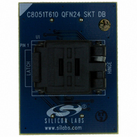
DAUGHTER BOARD T610 24QFN SOCKET
Manufacturer
Silicon Laboratories Inc
Datasheet
1.C8051T610DB32.pdf
(218 pages)
Specifications of C8051T610DB24
Module/board Type
Socket Module - QFN
Processor To Be Evaluated
C8051T61x
Interface Type
USB
Lead Free Status / RoHS Status
Lead free / RoHS Compliant
For Use With/related Products
C8051T610DK
Lead Free Status / RoHS Status
Lead free / RoHS Compliant, Lead free / RoHS Compliant
Other names
336-1507


C8051T610/1/2/3/4/5/6/7
14.1. Program Memory
The CIP-51 core has a 64 kB program memory space. The C8051T610/1/6/7 implements 15872 bytes of
this program memory space as in-system, Byte-Programmable EPROM, organized in a contiguous block
from addresses 0x0000 to 0x3FFF. Note that 512 bytes (0x3E00 – 0x3FFF) of this memory are reserved
for factory use and are not available for user program storage. The C8051T612/3/4/5 implements 8192
bytes of EPROM program memory space. Figure 14.2 shows the program memory maps for
C8051T610/1/2/3/4/5/6/7 devices.
Program memory is read-only from within firmware. Individual program memory bytes can be read using
the MOVC instruction. This facilitates the use of EPROM space for constant storage.
14.2. Data Memory
The C8051T610/1/2/3/4/5/6/7 device family includes 1280 bytes of RAM data memory. 256 bytes of this
memory is mapped into the internal RAM space of the 8051. 1024 bytes of this memory is on-chip “exter-
nal” memory. The data memory map is shown in Figure 14.1 for reference.
14.2.1. Internal RAM
There are 256 bytes of internal RAM mapped into the data memory space from 0x00 through 0xFF. The
lower 128 bytes of data memory are used for general purpose registers and scratch pad memory. Either
direct or indirect addressing may be used to access the lower 128 bytes of data memory. Locations 0x00
through 0x1F are addressable as four banks of general purpose registers, each bank consisting of eight
byte-wide registers. The next 16 bytes, locations 0x20 through 0x2F, may either be addressed as bytes or
as 128 bit locations accessible with the direct addressing mode.
The upper 128 bytes of data memory are accessible only by indirect addressing. This region occupies the
same address space as the Special Function Registers (SFR) but is physically separate from the SFR
space. The addressing mode used by an instruction when accessing locations above 0x7F determines
whether the CPU accesses the upper 128 bytes of data memory space or the SFRs. Instructions that use
direct addressing will access the SFR space. Instructions using indirect addressing above 0x7F access the
upper 128 bytes of data memory. Figure 14.1 illustrates the data memory organization of the
C8051T610/1/2/3/4/5/6/7.
78
C8051T610/1/6/7
EPROM Memory
Security Byte
15872 Bytes
Reserved
Figure 14.2. Program Memory Map
0x3FFF
0x3FFE
0x3E00
0x3DFF
0x0000
Rev 1.0
C8051T612/3/4/5
EPROM Memory
Security Byte
8192 Bytes
Reserved
0x3FFF
0x3FFE
0x2000
0x1FFF
0x0000
Related parts for C8051T610DB24
Image
Part Number
Description
Manufacturer
Datasheet
Request
R

Part Number:
Description:
SMD/C°/SINGLE-ENDED OUTPUT SILICON OSCILLATOR
Manufacturer:
Silicon Laboratories Inc
Part Number:
Description:
Manufacturer:
Silicon Laboratories Inc
Datasheet:
Part Number:
Description:
N/A N/A/SI4010 AES KEYFOB DEMO WITH LCD RX
Manufacturer:
Silicon Laboratories Inc
Datasheet:
Part Number:
Description:
N/A N/A/SI4010 SIMPLIFIED KEY FOB DEMO WITH LED RX
Manufacturer:
Silicon Laboratories Inc
Datasheet:
Part Number:
Description:
N/A/-40 TO 85 OC/EZLINK MODULE; F930/4432 HIGH BAND (REV E/B1)
Manufacturer:
Silicon Laboratories Inc
Part Number:
Description:
EZLink Module; F930/4432 Low Band (rev e/B1)
Manufacturer:
Silicon Laboratories Inc
Part Number:
Description:
I°/4460 10 DBM RADIO TEST CARD 434 MHZ
Manufacturer:
Silicon Laboratories Inc
Part Number:
Description:
I°/4461 14 DBM RADIO TEST CARD 868 MHZ
Manufacturer:
Silicon Laboratories Inc
Part Number:
Description:
I°/4463 20 DBM RFSWITCH RADIO TEST CARD 460 MHZ
Manufacturer:
Silicon Laboratories Inc
Part Number:
Description:
I°/4463 20 DBM RADIO TEST CARD 868 MHZ
Manufacturer:
Silicon Laboratories Inc
Part Number:
Description:
I°/4463 27 DBM RADIO TEST CARD 868 MHZ
Manufacturer:
Silicon Laboratories Inc
Part Number:
Description:
I°/4463 SKYWORKS 30 DBM RADIO TEST CARD 915 MHZ
Manufacturer:
Silicon Laboratories Inc
Part Number:
Description:
N/A N/A/-40 TO 85 OC/4463 RFMD 30 DBM RADIO TEST CARD 915 MHZ
Manufacturer:
Silicon Laboratories Inc
Part Number:
Description:
I°/4463 20 DBM RADIO TEST CARD 169 MHZ
Manufacturer:
Silicon Laboratories Inc