C8051T600SDB Silicon Laboratories Inc, C8051T600SDB Datasheet - Page 107
C8051T600SDB
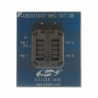
Manufacturer Part Number
C8051T600SDB
Description
BOARD SOCKET DAUGHTER SOIC
Manufacturer
Silicon Laboratories Inc
Datasheet
1.C8051T600EDB.pdf
(188 pages)
Specifications of C8051T600SDB
Module/board Type
Socket Module - SOIC
Data Bus Width
8 bit
Operating Supply Voltage
+ 1.8 V to + 3.6 V
Lead Free Status / RoHS Status
Contains lead / RoHS non-compliant
For Use With/related Products
C8051T600DK
Lead Free Status / Rohs Status
Lead free / RoHS Compliant
Other names
336-1405


22.1. Port I/O Modes of Operation
Port pins use the Port I/O cell shown in Figure 22.2. Each Port I/O cell can be configured by software for
analog I/O or digital I/O using the P0MDIN registers. On reset, all Port I/O cells default to a high impedance
state with weak pull-ups enabled until the crossbar is enabled (XBARE = 1).
22.1.1. Port Pins Configured for Analog I/O
Any pins to be used as inputs to the comparator, ADC, external oscillator, or VREF should be configured
for analog I/O (P0MDIN.n = 0). When a pin is configured for analog I/O, its weak pullup, digital driver, and
digital receiver are disabled. Port pins configured for analog I/O will always read back a value of 0.
Configuring pins as analog I/O saves power and isolates the Port pin from digital interference. Port pins
configured as digital inputs may still be used by analog peripherals; however, this practice is not recom-
mended and may result in measurement errors.
22.1.2. Port Pins Configured For Digital I/O
Any pins to be used by digital peripherals (UART, SMBus, PCA, etc.), external digital event capture func-
tions, or as GPIO should be configured as digital I/O (P0MDIN.n = 1). For digital I/O pins, one of two output
modes (push-pull or open-drain) must be selected using the P0MDOUT registers.
Push-pull outputs (P0MDOUT.n = 1) drive the Port pad to the VDD or GND supply rails based on the out-
put logic value of the Port pin. Open-drain outputs have the high side driver disabled; therefore, they only
drive the Port pad to GND when the output logic value is 0 and become high impedance inputs (both high
and low drivers turned off) when the output logic value is 1.
When a digital I/O cell is placed in the high impedance state, a weak pull-up transistor pulls the Port pad to
the VDD supply voltage to ensure the digital input is at a defined logic state. Weak pull-ups are disabled
when the I/O cell is driven to GND to minimize power consumption and may be globally disabled by setting
WEAKPUD to 1. The user should ensure that digital I/O are always internally or externally pulled or driven
to a valid logic state to minimize power consumption. Port pins configured for digital I/O always read back
the logic state of the Port pad, regardless of the output logic value of the Port pin.
WEAKPUD
(Weak Pull-Up Disable)
Px.x – Output
Logic Value
(Port Latch or
Crossbar)
PxMDOUT.x
(1 for push-pull)
(0 for open-drain)
XBARE
(Crossbar
Enable)
Px.x – Input Logic Value
(Reads 0 when pin is configured as an analog I/O)
To/From Analog
Peripheral
PxMDIN.x
(1 for digital)
(0 for analog)
Figure 22.2. Port I/O Cell Block Diagram
Rev. 1.2
C8051T600/1/2/3/4/5/6
VDD
GND
VDD
(WEAK)
PORT
PAD
107
Related parts for C8051T600SDB
Image
Part Number
Description
Manufacturer
Datasheet
Request
R

Part Number:
Description:
SMD/C°/SINGLE-ENDED OUTPUT SILICON OSCILLATOR
Manufacturer:
Silicon Laboratories Inc
Part Number:
Description:
Manufacturer:
Silicon Laboratories Inc
Datasheet:
Part Number:
Description:
N/A N/A/SI4010 AES KEYFOB DEMO WITH LCD RX
Manufacturer:
Silicon Laboratories Inc
Datasheet:
Part Number:
Description:
N/A N/A/SI4010 SIMPLIFIED KEY FOB DEMO WITH LED RX
Manufacturer:
Silicon Laboratories Inc
Datasheet:
Part Number:
Description:
N/A/-40 TO 85 OC/EZLINK MODULE; F930/4432 HIGH BAND (REV E/B1)
Manufacturer:
Silicon Laboratories Inc
Part Number:
Description:
EZLink Module; F930/4432 Low Band (rev e/B1)
Manufacturer:
Silicon Laboratories Inc
Part Number:
Description:
I°/4460 10 DBM RADIO TEST CARD 434 MHZ
Manufacturer:
Silicon Laboratories Inc
Part Number:
Description:
I°/4461 14 DBM RADIO TEST CARD 868 MHZ
Manufacturer:
Silicon Laboratories Inc
Part Number:
Description:
I°/4463 20 DBM RFSWITCH RADIO TEST CARD 460 MHZ
Manufacturer:
Silicon Laboratories Inc
Part Number:
Description:
I°/4463 20 DBM RADIO TEST CARD 868 MHZ
Manufacturer:
Silicon Laboratories Inc
Part Number:
Description:
I°/4463 27 DBM RADIO TEST CARD 868 MHZ
Manufacturer:
Silicon Laboratories Inc
Part Number:
Description:
I°/4463 SKYWORKS 30 DBM RADIO TEST CARD 915 MHZ
Manufacturer:
Silicon Laboratories Inc
Part Number:
Description:
N/A N/A/-40 TO 85 OC/4463 RFMD 30 DBM RADIO TEST CARD 915 MHZ
Manufacturer:
Silicon Laboratories Inc
Part Number:
Description:
I°/4463 20 DBM RADIO TEST CARD 169 MHZ
Manufacturer:
Silicon Laboratories Inc