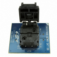
C8051T600QDB Silicon Laboratories Inc, C8051T600QDB Datasheet - Page 97

C8051T600QDB
Manufacturer Part Number
C8051T600QDB
Description
BOARD SOCKET DAUGHTER QFN
Manufacturer
Silicon Laboratories Inc
Datasheet
1.C8051T600EDB.pdf
(188 pages)
Specifications of C8051T600QDB
Module/board Type
Socket Module - QFN
Data Bus Width
8 bit
Operating Supply Voltage
+ 1.8 V to + 3.6 V
Lead Free Status / RoHS Status
Contains lead / RoHS non-compliant
For Use With/related Products
C8051T600DK
Lead Free Status / Rohs Status
Lead free / RoHS Compliant
Other names
336-1406
- Current page: 97 of 188
- Download datasheet (898Kb)
C8051T600/1/2/3/4/5/6
20. EPROM Memory
Electrically programmable read-only memory (EPROM) is included on-chip for program code storage. The
EPROM memory can be programmed via the C2 debug and programming interface when a special pro-
gramming voltage is applied to the V
pin. Each location in EPROM memory is programmable only once
PP
(i.e., non-erasable). Table 8.6 on page 34 shows the EPROM specifications.
20.1. Programming and Reading the EPROM Memory
Reading and writing the EPROM memory is accomplished through the C2 programming and debug inter-
face. When creating hardware to program the EPROM, it is necessary to follow the programming steps
listed below. Refer to the “C2 Interface Specification” available at http://www.silabs.com for details on com-
municating via the C2 interface. Section “27. C2 Interface” on page 178 has information about C2 register
addresses for the C8051T600/1/2/3/4/5/6.
20.1.1. EPROM Write Procedure
1. Reset the device using the RST pin.
2. Wait at least 20 µs before sending the first C2 command.
3. Place the device in core reset: Write 0x04 to the DEVCTL register.
4. Set the device to program mode (1st step): Write 0x40 to the EPCTL register.
5. Set the device to program mode (2nd step): Write 0x58 to the EPCTL register.
6. Apply the VPP programming Voltage.
7. Write the first EPROM address for programming to EPADDRH and EPADDRL.
8. Write a data byte to EPDAT. EPADDRH:L will increment by 1 after this write.
9. Use a C2 Address Read command to poll for write completion.
10.(Optional) Check the ERROR bit in register EPSTAT and abort the programming operation if necessary.
11. If programming is not finished, return to Step 8 to write the next address in sequence, or return to
Step 7 to program a new address.
12.Remove the VPP programming Voltage.
13.Remove program mode (1st step): Write 0x40 to the EPCTL register.
14.Remove program mode (2nd step): Write 0x00 to the EPCTL register.
15.Reset the device: Write 0x02 and then 0x00 to the DEVCTL register.
Important Note: There is a finite amount of time which V
can be applied without damaging the device,
PP
which is cumulative over the life of the device. Refer to Table 8.1 on page 30 for the V
timing specifica-
PP
tion.
Rev. 1.2
97
Related parts for C8051T600QDB
Image
Part Number
Description
Manufacturer
Datasheet
Request
R
Part Number:
Description:
SMD/C°/SINGLE-ENDED OUTPUT SILICON OSCILLATOR
Manufacturer:
Silicon Laboratories Inc
Part Number:
Description:
Manufacturer:
Silicon Laboratories Inc
Datasheet:
Part Number:
Description:
N/A N/A/SI4010 AES KEYFOB DEMO WITH LCD RX
Manufacturer:
Silicon Laboratories Inc
Datasheet:
Part Number:
Description:
N/A N/A/SI4010 SIMPLIFIED KEY FOB DEMO WITH LED RX
Manufacturer:
Silicon Laboratories Inc
Datasheet:
Part Number:
Description:
N/A/-40 TO 85 OC/EZLINK MODULE; F930/4432 HIGH BAND (REV E/B1)
Manufacturer:
Silicon Laboratories Inc
Part Number:
Description:
EZLink Module; F930/4432 Low Band (rev e/B1)
Manufacturer:
Silicon Laboratories Inc
Part Number:
Description:
I°/4460 10 DBM RADIO TEST CARD 434 MHZ
Manufacturer:
Silicon Laboratories Inc
Part Number:
Description:
I°/4461 14 DBM RADIO TEST CARD 868 MHZ
Manufacturer:
Silicon Laboratories Inc
Part Number:
Description:
I°/4463 20 DBM RFSWITCH RADIO TEST CARD 460 MHZ
Manufacturer:
Silicon Laboratories Inc
Part Number:
Description:
I°/4463 20 DBM RADIO TEST CARD 868 MHZ
Manufacturer:
Silicon Laboratories Inc
Part Number:
Description:
I°/4463 27 DBM RADIO TEST CARD 868 MHZ
Manufacturer:
Silicon Laboratories Inc
Part Number:
Description:
I°/4463 SKYWORKS 30 DBM RADIO TEST CARD 915 MHZ
Manufacturer:
Silicon Laboratories Inc
Part Number:
Description:
N/A N/A/-40 TO 85 OC/4463 RFMD 30 DBM RADIO TEST CARD 915 MHZ
Manufacturer:
Silicon Laboratories Inc
Part Number:
Description:
I°/4463 20 DBM RADIO TEST CARD 169 MHZ
Manufacturer:
Silicon Laboratories Inc


