C8051T610DB28 Silicon Laboratories Inc, C8051T610DB28 Datasheet - Page 117
C8051T610DB28
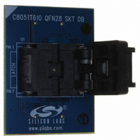
Manufacturer Part Number
C8051T610DB28
Description
DAUGHTER BOARD T610 28QFN SOCKET
Manufacturer
Silicon Laboratories Inc
Datasheet
1.C8051T610DB32.pdf
(218 pages)
Specifications of C8051T610DB28
Module/board Type
Socket Module - QFN
Processor To Be Evaluated
C8051T61x
Interface Type
USB
Lead Free Status / RoHS Status
Lead free / RoHS Compliant
For Use With/related Products
C8051T610DK
Lead Free Status / RoHS Status
Lead free / RoHS Compliant, Lead free / RoHS Compliant
Other names
336-1506


21.2.3. Assigning Port I/O Pins to INT0 or INT1 external interrupts
INT0 and INT1 can be used to trigger an interrupt on any Port 0 I/O pin. These functions do not require
dedicated pins, meaning that they can function on both GPIO pins (PnSKIP = 1) and pins in use by the
crossbar (PnSKIP = 0). INT0 and INT1 cannot be used on pins configured for analog I/O. Table 21.3 shows
the available external digital event capture functions.
21.3. Priority Crossbar Decoder
The Priority Crossbar Decoder (Figure 21.3) assigns a priority to each I/O function, starting at the top with
UART0. When a digital resource is selected, the least-significant unassigned Port pin is assigned to that
resource (excluding UART0, which is always at pins 4 and 5). If a Port pin is assigned, the Crossbar skips
that pin when assigning the next selected resource. Additionally, the Crossbar will skip Port pins whose
associated bits in the PnSKIP registers are set. The PnSKIP registers allow software to skip Port pins that
are to be used for analog input, dedicated functions, or GPIO.
Important Note on Crossbar Configuration: If a Port pin is claimed by a peripheral without use of the
Crossbar, its corresponding PnSKIP bit should be set. This applies to P0.0 if VREF is used, P0.3 if the
external oscillator circuit is enabled, P0.6 if the ADC is configured to use the external conversion start sig-
nal (CNVSTR), and any selected ADC or Comparator inputs. The Crossbar skips selected pins as if they
were already assigned, and moves to the next unassigned pin. Figure 21.3 shows the potential pin assig-
ments available to the crossbar peripherals. Figure 21.4 and Figure 21.5 show two example crossbar con-
figurations, with and without skipping pins.
Registers XBR0 and XBR1 are used to assign the digital I/O resources to the physical I/O Port pins. Note
that when a peripheral is selected, the crossbar assigns all pins for that peripheral. UART0 pin assign-
ments are fixed for bootloading purposes: UART TX0 is always assigned to P0.4; UART RX0 is always
assigned to P0.5. Standard Port I/Os appear contiguously after the prioritized functions have been
assigned.
Important Note: The SPI can be operated in either 3-wire or 4-wire modes, pending the state of the
NSSMD1–NSSMD0 bits in register SPI0CN. According to the SPI mode, the NSS signal may or may not
be routed to a Port pin.
Digital Function
External Interrupt 0 (INT0)
External Interrupt 1 (INT1)
Table 21.3. Port I/O Assignment for INT0 and INT1 Functions
Potentially Assignable Port Pins
Rev 1.0
P0.0–P0.7
P0.0–P0.7
C8051T610/1/2/3/4/5/6/7
SFR(s) used for
Assignment
IT01CF
IT01CF
117
Related parts for C8051T610DB28
Image
Part Number
Description
Manufacturer
Datasheet
Request
R

Part Number:
Description:
SMD/C°/SINGLE-ENDED OUTPUT SILICON OSCILLATOR
Manufacturer:
Silicon Laboratories Inc
Part Number:
Description:
Manufacturer:
Silicon Laboratories Inc
Datasheet:
Part Number:
Description:
N/A N/A/SI4010 AES KEYFOB DEMO WITH LCD RX
Manufacturer:
Silicon Laboratories Inc
Datasheet:
Part Number:
Description:
N/A N/A/SI4010 SIMPLIFIED KEY FOB DEMO WITH LED RX
Manufacturer:
Silicon Laboratories Inc
Datasheet:
Part Number:
Description:
N/A/-40 TO 85 OC/EZLINK MODULE; F930/4432 HIGH BAND (REV E/B1)
Manufacturer:
Silicon Laboratories Inc
Part Number:
Description:
EZLink Module; F930/4432 Low Band (rev e/B1)
Manufacturer:
Silicon Laboratories Inc
Part Number:
Description:
I°/4460 10 DBM RADIO TEST CARD 434 MHZ
Manufacturer:
Silicon Laboratories Inc
Part Number:
Description:
I°/4461 14 DBM RADIO TEST CARD 868 MHZ
Manufacturer:
Silicon Laboratories Inc
Part Number:
Description:
I°/4463 20 DBM RFSWITCH RADIO TEST CARD 460 MHZ
Manufacturer:
Silicon Laboratories Inc
Part Number:
Description:
I°/4463 20 DBM RADIO TEST CARD 868 MHZ
Manufacturer:
Silicon Laboratories Inc
Part Number:
Description:
I°/4463 27 DBM RADIO TEST CARD 868 MHZ
Manufacturer:
Silicon Laboratories Inc
Part Number:
Description:
I°/4463 SKYWORKS 30 DBM RADIO TEST CARD 915 MHZ
Manufacturer:
Silicon Laboratories Inc
Part Number:
Description:
N/A N/A/-40 TO 85 OC/4463 RFMD 30 DBM RADIO TEST CARD 915 MHZ
Manufacturer:
Silicon Laboratories Inc
Part Number:
Description:
I°/4463 20 DBM RADIO TEST CARD 169 MHZ
Manufacturer:
Silicon Laboratories Inc