KSZ8851SNL-BBE-EVAL Micrel Inc, KSZ8851SNL-BBE-EVAL Datasheet
KSZ8851SNL-BBE-EVAL
Specifications of KSZ8851SNL-BBE-EVAL
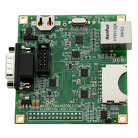
KSZ8851SNL-BBE-EVL
ZIPPY2
Available stocks


Related parts for KSZ8851SNL-BBE-EVAL


KSZ8851SNL-BBE-EVAL Summary of contents
Page 1
... TX (allocated 6KB) and RX (allocated 12KB) directions in host buffer interface. The KSZ8851SNL is designed to be fully compliant with the appropriate IEEE 802.3 standards. An industrial temperature-grade version of the KSZ8851SNL, the KSZ8851SNLI is also available (see “Ordering Information” ...
Page 2
... Available in 32-pin (5mm x 5mm) MLF August 2009 Additional Features In addition to offering all of the features of a Layer 2 controller, the KSZ8851SNL offers: • Supports to add two-byte before frame header in order for IP frame content with double word boundary • Micrel LinkMD determine cable length, diagnose faulty cables, and determine distance to fault • ...
Page 3
... Micrel, Inc. Ordering Information Part Number Temperature Range KSZ8851SNL TR KSZ8851SNLI TR –40 KSZ8851SNL-Eval Evaluation Board for the KSZ8851SNL Revision History Revision Date 1.0 06/30/2008 1.1 2/13/2009 2.0 8/31/2009 August 2009 Package 32-Pin MLF +85 C 32-Pin MLF Summary of Changes First released Information. Improved EDS Rating up to 6KV, revised Ordering Information and updated Table content and description ...
Page 4
... Half-Duplex Backpressure ....................................................................................................................................... 21 Address Filtering Function ....................................................................................................................................... 21 Clock Generator ....................................................................................................................................................... 22 Serial Peripheral Interface (SPI) ..................................................................................................................................... 22 SPI Internal I/O Registers Access Operation Timing............................................................................................... 23 SPI TXQ/RXQ FIFOs Access Operation Timing...................................................................................................... 23 Queue Management Unit (QMU).................................................................................................................................... 24 Transmit Queue (TXQ) Frame Format..................................................................................................................... 24 Frame Transmitting Path Operation in TXQ ............................................................................................................ 25 August 2009 4 KSZ8851SNL/SNLI M9999-083109-2.0 ...
Page 5
... Micrel, Inc. Driver Routine for Transmit Packet from Host Processor to KSZ8851SNL............................................................. 26 Receive Queue (RXQ) Frame Format ..................................................................................................................... 29 Frame Receiving Path Operation in RXQ ................................................................................................................ 29 Driver Routine for Receive Packet from KSZ8851SNL to Host Processor.............................................................. 30 EEPROM Interface ......................................................................................................................................................... 31 Loopback Support........................................................................................................................................................... 32 Near-end (Remote) Loopback.................................................................................................................................. 32 Far-end (Local) Loopback ........................................................................................................................................ 32 SPI Interface to I/O Registers............................................................................................................................................. 33 I/O Registers ...
Page 6
... Flow Control Overrun Watermark Register (0xB4 – 0xB5): FCOWR............................................................................. 59 0xB6 – 0xBF: Reserved.................................................................................................................................................. 59 Chip ID and Enable Register (0xC0 – 0xC1): CIDER .................................................................................................... 59 0xC2 – 0xC5: Reserved ................................................................................................................................................. 59 Chip Global Control Register (0xC6 – 0xC7): CGCR..................................................................................................... 59 Indirect Access Control Register (0xC8 – 0xC9): IACR ................................................................................................. 59 0xCA – 0xCF: Reserved ................................................................................................................................................. 60 August 2009 6 KSZ8851SNL/SNLI M9999-083109-2.0 ...
Page 7
... MIB (Management Information Base) Counters............................................................................................................... 69 Additional MIB Information ............................................................................................................................................. 70 Absolute Maximum Ratings ............................................................................................................................................... 71 Operating Ratings ............................................................................................................................................................... 71 Electrical Characteristics ................................................................................................................................................... 71 Timing Specifications ......................................................................................................................................................... 73 SPI Input and Output Timing .......................................................................................................................................... 73 Auto Negotiation Timing ................................................................................................................................................. 74 Reset Timing................................................................................................................................................................... 75 EEPROM Timing ............................................................................................................................................................ 76 Selection of Isolation Transformers.................................................................................................................................. 77 Selection of Reference Crystal .......................................................................................................................................... 77 Package Information ........................................................................................................................................................... 78 Acronyms and Glossary..................................................................................................................................................... 79 August 2009 7 KSZ8851SNL/SNLI M9999-083109-2.0 ...
Page 8
... Figure 2. 32-Pin (5mm x 5mm) MLF Figure 3. Typical Straight Cable Connection ........................................................................................................................ 17 Figure 4. Typical Crossover Cable Connection .................................................................................................................... 18 Figure 5. Auto Negotiation and Parallel Operation ............................................................................................................... 19 Figure 6. SPI Interface to KSZ8851SNL ............................................................................................................................... 22 Figure 7. Internal I/O Register Read Timing ......................................................................................................................... 23 Figure 8. Internal I/O Register Write Timing ......................................................................................................................... 23 Figure 9. RXQ FIFO Read Timing......................................................................................................................................... 24 Figure 10 ...
Page 9
... Table 8. Transmit Byte Count Format................................................................................................................................... 25 Table 9. Registers Setting for Transmit Function Block........................................................................................................ 26 Table 10. Frame Format for Receive Queue ........................................................................................................................ 29 Table 11. Registers Setting for Receive Function Block....................................................................................................... 29 Table 12. KSZ8851SNL EEPROM Format ........................................................................................................................... 31 Table 13. Format of MIB Counters........................................................................................................................................ 69 Table 14. Port 1 MIB Counters Indirect Memory Offsets ...................................................................................................... 70 Table 15. Electrical Characteristics....................................................................................................................................... 72 Table 16 ...
Page 10
... Micrel, Inc. Pin Configuration August 2009 Figure 2. 32-Pin (5mm x 5mm) MLF 10 KSZ8851SNL/SNLI ® M9999-083109-2.0 ...
Page 11
... Speed = LED On (100BASE-T); LED Off (10BASE-T) Power Management Event (default active low asserted (low or high depends on polarity set in PMECR register) when one of the wake-on-LAN events is detected by KSZ8851SNL. The KSZ8851SNL is requesting the system to wake up from low power mode. Interrupt Not An active low signal to host CPU to indicate an interrupt status bit is set. This pin needs an external 4 ...
Page 12
... EEPROM select: Pull-up = EEPROM present Floating (NC) or Pull-down = EEPROM not present (default) During power-up / reset, this pin value is latched into register CCR, bit 9 12 input power supply for IO with well decoupling capacitors. input power supply for IO with well decoupling capacitors. KSZ8851SNL/SNLI M9999-083109-2.0 ...
Page 13
... Normal Operation Mode This is the default setting bit[1:0]=00 in PMECR register after the chip power-up or hardware reset (pin 67). When KSZ8851SNL is in this normal operation mode, all PLL clocks are running, PHY and MAC are on and the host interface is ready for CPU read or write. ...
Page 14
... Once the power management unit detects the PME output asserted or interrupt active, it will power up the host CPU and issue a wakeup command which is any one of registers read or write access to wake up the KSZ8851SNL from the low power state to the normal power state in case the auto-wakeup enable bit[7] is disabled. When KSZ8851SNL is at normal power state able to transmit or receive packet from the cable ...
Page 15
... If the LAN controller scans a frame and does not find the specific sequence shown above, it discards the frame and takes no further action. If the KSZ8851SNL controller detects the data sequence, however, it then alerts the PC’s power management circuitry (assert the PME pin) to wake up the system. ...
Page 16
... RXP or RXM input from falsely triggering the decoder. When the input exceeds the squelch limit, the PLL locks onto the incoming signal and the KSZ8851SNL decodes a data frame. The receiver clock is maintained active during idle periods in between data reception. ...
Page 17
... The auto-sense function detects remote transmit and receive pairs and correctly assigns the transmit and receive pairs for the KSZ8851SNL device. This feature is extremely useful when end users are unaware of cable types in addition to saving on an additional uplink configuration connection. The auto-crossover feature can be disabled through the port control registers ...
Page 18
... If auto negotiation is not supported or the link partner to the KSZ8851SNL is forced to bypass auto negotiation, the mode is set by observing the signal at the receiver. This is known as parallel mode because while the transmitter is sending auto negotiation advertisements, the receiver is listening for advertisements or a fixed signal protocol ...
Page 19
... Set Link Mode ® LinkMD Cable Diagnostics ® The KSZ8851SNL LinkMD uses time domain reflectometry (TDR) to analyze the cabling plant for common cabling problems such as open circuits, short circuits, and impedance mismatches. ® LinkMD works by sending a pulse of known amplitude and duration down the MDI and MDI-X pairs and then analyzes the shape of the reflected signal. Timing the pulse duration gives an indication of the distance to the cabling fault with a maximum distance of 200m and an accuracy of ± ...
Page 20
... If P1SCLMD[14:13]=11, this indicates an invalid test, and occurs when the KSZ8851SNL is unable to shut down the link partner. In this instance, the test is not run not possible for the KSZ8851SNL to determine if the detected signal is a reflection of the signal generated or a signal from another source. ...
Page 21
... Physical address 1 passed Note 1: Bit 0 (RX Enable), Bit 5 (RX Unicast Enable) and Bit 6 (RX Multicast Enable) must set RXCR1 register. Note 2: The KSZ8851SNL will discard frame with SA same as the MAC address if bit[0] is set in RXCR2 register. August 2009 RX Physical RX Multicast Address Address ...
Page 22
... CPU) supplies the operating serial clock (SCLK), chip select (CSN) and serial input data (SI) which is clocked in on the rising edge of SCLK to KSZ8851SNL device. Serial output data (SO) is driven out by the KSZ8851SNL on the falling edge of SCLK to external SPI master device. The falling edge of CSN is starting the SPI operation and the rising edge of CSN is ending the SPI operation ...
Page 23
... Opcode Don’t care bits Table 5. SPI Operation for TXQ/RXQ FIFO Access Figure 7. Internal I/O Register Read Timing Figure 8. Internal I/O Register Write Timing 23 KSZ8851SNL/SNLI Data Phase ( pins KBytes (DMA read data on SO pin KBytes (DMA write data on SI pin) M9999-083109-2.0 ...
Page 24
... The frame format for the transmit queue is shown in the following Table 6. The first word contains the control information August 2009 Read Data Byte Read Data Byte 4 Figure 9. RXQ FIFO Read Timing Figure 10. TXQ FIFO Write Timing Read Data Byte Read Data Byte N KSZ8851SNL/SNLI M9999-083109-2.0 ...
Page 25
... The data area contains six bytes of Destination Address (DA) followed by six bytes of Source Address (SA), followed by a variable-length number of bytes. On transmit, all bytes are provided by the CPU, including the source address. The KSZ8851SNL does not insert its own SA. The 802.3 Frame Length word (Frame Type in Ethernet) is not interpreted by the KSZ8851SNL treated transparently as data both for transmit operations. ...
Page 26
... Note: This bit is self-clearing after the frame is finished transmitting. The software should wait for the bit to be cleared before setting up another new TX frame. TXQCR[1](0x80) When this bit is written as 1, the KSZ8851SNL will generate interrupt (bit 6 in ISR register) to CPU when TXQ memory is available based upon the total amount of TXQ space requested by CPU at TXNTFSR (0x9E) register. ...
Page 27
... TXQ write access, then Host issues a SPI opcode=11 to start write transmit data (control word, byte count and pkt data) to TXQ memory. This is moving transmit data from Host to KSZ8851SNL TXQ memory until whole pkt is finished Write an 0?to RXQCR[3] reg to end Write an 1?to TXQCR[0] reg to issue a transmit command (manual-enqueue) to the TXQ ...
Page 28
... SPI opcode=11 to start write transmit data (control word, byte count and pkt data) to TXQ memory. This is moving transmit data from Host to KSZ8851SNL TXQ memory until all pkts are finished Write an 0?to RXQCR[3] reg to end TXQ write access Option to read ISR[14] reg, it indicates ...
Page 29
... Set bit 14 to enable RXQ address register increments automatically on accesses to the data register. RXDTTR[15:0](0x8C) To program received frame duration timer value. When Rx frame duration in RXQ exceeds this threshold interval count and bit 7 of RXQCR register is set to 1, the KSZ8851SNL will generate RX interrupt in ISR[13] and indicate the status in RXQCR[12]. RXDBCTR[15:0](0x8E) To program received data byte count value ...
Page 30
... Driver Routine for Receive Packet from KSZ8851SNL to Host Processor The software driver receives data packet frames from the KSZ8851SNL device either as a result of polling or an interrupt based service. When an interrupt is received, the OS invokes the interrupt service routine that is in the interrupt vector table ...
Page 31
... EEPROM Interface It is optional in the KSZ8851SNL to use an external EEPROM. The EED_IO (pin 6) must be pulled high to use external EEPROM otherwise this pin pulled low or floating without EEPROM. An external serial EEPROM with a standard microwire bus interface is used for non-volatile storage of information such as the host MAC address ...
Page 32
... Figure 14. Far-end (Local) Loopback Far-end (Local) loopback is conducted at Host of the KSZ8851SNL. The loopback path starts at the host SPI FIFO write to transmit data, wraps around at the PHY port’s PMD/PMA, and ends at the host SPI FIFO read to receive data. Bit [14] of register P1MBCR (0xE4) is used to enable far-end loopback at host side. The host far-end loopback path is illustrated in the following Figure 14 ...
Page 33
... Micrel, Inc. SPI Interface to I/O Registers The KSZ8851SNL provides a SPI interface for the host CPU to access its internal I/O registers. I/O registers serve as the address that the microprocessor uses when communicating with the device. This is used for configuring operational settings, reading or writing control, status information, and transferring packets. ...
Page 34
... WFCR 0x0000 0x2B 0x2C 0x2D Don’t care Reserved 0x2E 0x2F 34 KSZ8851SNL/SNLI Description None None Chip Configuration Register [7:0] Chip Configuration Register [15:8] None None MAC Address Register Low [7:0] MAC Address Register Low [15:8] MAC Address Register Middle [7:0] ...
Page 35
... Reserved Don’t care 0x5E 0x5F 35 KSZ8851SNL/SNLI Description Wakeup Frame 0 CRC0 Register [7:0] Wakeup Frame 0 CRC0 Register [15:8] Wakeup Frame 0 CRC1 Register [7:0] Wakeup Frame 0 CRC1 Register [15:8] Wakeup Frame 0 Byte Mask 0 Register [7:0] Wakeup Frame 0 Byte Mask 0 Register [15:8] ...
Page 36
... RXDTTR 0x0000 0x8D 0x8E RXDBCTR 0x0000 0x8F 36 KSZ8851SNL/SNLI Description Wakeup Frame 3 CRC0 Register [7:0] Wakeup Frame 3 CRC0 Register [15:8] Wakeup Frame 3 CRC1 Register [7:0] Wakeup Frame 3 CRC1 Register [15:8] Wakeup Frame 3 Byte Mask 0 Register [7:0] Wakeup Frame 3 Byte Mask 0 Register [15:8] ...
Page 37
... Reserved Don’t care 0xBE 0xBF 37 KSZ8851SNL/SNLI Description Interrupt Enable Register [7:0] Interrupt Enable Register [15:8] Interrupt Status Register [7:0] Interrupt Status Register [15:8] None None RX Frame Count & Threshold Register [7:0] RX Frame Count & Threshold Register [15:8] ...
Page 38
... P1ANAR 0x05E1 0xED 0xEE P1ANLPR 0x0001 0xEF 38 KSZ8851SNL/SNLI Description Chip ID and Enable Register [7:0] Chip ID and Enable Register [15:8] None None Chip Global Control Register [7:0] Chip Global Control Register [15:8] Indirect Access Control Register [7:0] Indirect Access Control Register [15:8] ...
Page 39
... Don’t care 0xFB 0xFC 0xFD Reserved Don’t care 0xFE 0xFF 39 KSZ8851SNL/SNLI Description None Port 1 PHY Special Control/Status, LinkMD Port 1 PHY Special Control/Status, LinkMD Port 1 Control Register [7:0] Port 1 Control Register [15:8] Port 1 Status Register [7:0] Port 1 Status Register [15:8] ...
Page 40
... MARM[15:0] = EEPROM 0x2(MAC Byte 4 and 3) MARH[15:0] = EEPROM 0x3(MAC Byte 6 and 5) The Host MAC address is used to define the individual destination address that the KSZ8851SNL responds to when receiving frames. Network addresses are generally expressed in the form of 01:23:45:67:89:AB, where the bytes are received from left to right, and the bits within each byte are received from right to left (LSB to MSB). For example, the actual transmitted and received bits are on the order of 10000000 11000100 10100010 11100110 10010001 11010101 ...
Page 41
... On-Chip Bus Control Register (0x20 – 0x21): OBCR This register controls the on-chip bus clock speed for the KSZ8851SNL. The default of the on-chip bus clock speed is 125 MHz. When the external host CPU is running at a higher clock rate, the on-chip bus should be adjusted for the best performance ...
Page 42
... EEPROM is not used, the software programs the host MAC address EEPROM is used in the design, the chip host MAC address is loaded from the EEPROM immediately after reset. The KSZ8851SNL allows the software to access (read and write) the EEPROM directly; that is, the EEPROM access timing can be fully controlled by the software if the EEPROM Software Access bit is set ...
Page 43
... Wake up Frame 1 Enable When set, it enables the Wake up frame 1 pattern detection. When reset, the Wake up frame 1 pattern detection is disabled. WF0E Wake up Frame 0 Enable When set, it enables the Wake up frame 0 pattern detection. When reset, the Wake up frame 0 pattern detection is disabled. 43 KSZ8851SNL/SNLI M9999-083109-2.0 ...
Page 44
... The next 16 bytes mask covering bytes Wake up frame 0 pattern. Description WF0BM2 Wake-up Frame 0 Byte Mask 2. The next 16 bytes mask covering bytes Wake-up frame 0 pattern. Description WF0BM3 Wake-up Frame 0 Byte Mask 3. The last 16 bytes mask covering bytes Wake-up frame 0 pattern. 44 KSZ8851SNL/SNLI M9999-083109-2.0 ...
Page 45
... Wake-up frame 1 Byte Mask 0. The first 16 bytes mask of a Wake-up frame 1 pattern. Description WF1BM1 Wake-up frame 1 Byte Mask 1. The next 16 bytes mask covering bytes Wake-up frame 1 pattern. Description WF1BM2 Wake-up frame 1 Byte Mask 2. The next 16 bytes mask covering bytes Wake-up frame 1 pattern. 45 KSZ8851SNL/SNLI M9999-083109-2.0 ...
Page 46
... Wake-up frame 2 Byte Mask 0. The first 16 bytes mask of a Wake-up frame 2 pattern. Description WF2BM1 Wake-up frame 2 Byte Mask 1. The next 16 bytes mask covering bytes Wake-up frame 2 pattern. Description WF2BM2 Wake-up frame 2 Byte Mask 2. The next 16 bytes mask covering bytes Wake-up frame 2 pattern. 46 KSZ8851SNL/SNLI M9999-083109-2.0 ...
Page 47
... Wake up Frame 3 Byte Mask 0. The first 16 byte mask of a Wake up frame 3 pattern. Description WF3BM1 Wake up Frame 3 Byte Mask 1. The next 16 bytes mask covering bytes Wake up frame 3 pattern. Description WF3BM2 Wake up Frame 3 Byte Mask 2. The next 16 bytes mask covering bytes Wake up frame 3 pattern. 47 KSZ8851SNL/SNLI M9999-083109-2.0 ...
Page 48
... Wake up frame 3 pattern. Description Reserved TCGICMP Transmit Checksum Generation for ICMP When this bit is set, The KSZ8851SNL is enabled to transmit ICMP frame (only for non- fragment frame) checksum generation. Reserved TCGTCP Transmit Checksum Generation for TCP When this bit is set, The KSZ8851SNL is enabled to transmit TCP frame checksum generation ...
Page 49
... RXFCE Receive Flow Control Enable When this bit is set and the KSZ8851SNL is in full-duplex mode, flow control is enabled, and the KSZ8851SNL will acknowledge a PAUSE frame from the receive interface; i.e., the outgoing packets are pending in the transmit buffer until the PAUSE frame control timer expires ...
Page 50
... Note: It needs RXQ FIFO Read command byte before each data burst. IUFFP IPV4/IPV6/UDP Fragment Frame Pass When this bit is set, the KSZ8851SNL will pass the checksum check at receive side for IPv4/IPv6 UDP frame with fragment extension header. When this bit is cleared, the KSZ8851SNL will perform checksum operation based on configuration and doesn’ ...
Page 51
... ICMP frames (only for non-fragment frame). Any received ICMP frames with incorrect checksum will be discarded. RXSAF Receive Source Address Filtering When this bit is set, the KSZ8851SNL will drop the frame if the source address is same as MAC address in MARL, MARM, MARH registers. Description ...
Page 52
... The bit 0 METFE has to be set 0 when this bit is set this register. TXQMAM TXQ Memory Available Monitor When this bit is written as 1, the KSZ8851SNL will generate interrupt (bit 6 in ISR register) to CPU when TXQ memory is available based upon the total amount of TXQ space requested by CPU at TXNTFSR (0x9E) register ...
Page 53
... This bit will be updated when write 1 to bit 13 in ISR register. RXIPHTOE RX IP Header Two-Byte Offset Enable When this bit is written as 1, the KSZ8851SNL will enable to add two bytes before frame header in order for IP header inside the frame contents to be aligned with double word boundary to speed up software operation ...
Page 54
... When this bit is reset, the RX frame data pointer is manually controlled by user to access the RX frame location. Reserved RXFP RX Frame Pointer RX Frame data pointer index to the Data register for access. This pointer value must reset to 0x000 before each DMA operation from the host CPU to read RXQ frame buffer. 54 KSZ8851SNL/SNLI M9999-083109-2.0 ...
Page 55
... To program received frame duration timer threshold value in 1us interval. The maximum value is 0xCFFF. When bit 7 set RXQCR register, the KSZ8851SNL will set RX interrupt (bit 13 in ISR) after the time starts at first received frame in RXQ buffer and exceeds the threshold set in this register. ...
Page 56
... When this bit is set, it indicates that the Transmit Process has stopped. This edge-triggered interrupt status is cleared by writing 1 to this bit. RXPSIS Receive Process Stopped Interrupt Status When this bit is set, it indicates that the Receive Process has stopped. This edge-triggered interrupt status is cleared by writing 1 to this bit. Reserved 56 KSZ8851SNL/SNLI M9999-083109-2.0 ...
Page 57
... RX frame count register. RXFCT Receive Frame Count Threshold To program received frame count threshold value. When bit 5 set RXQCR register, the KSZ8851SNL will set RX interrupt (bit 13 in ISR) when the number of received frames in RXQ buffer exceeds the threshold set in this register. ...
Page 58
... Description Reserved FCLWC Flow Control Low Watermark Configuration These bits are used to define the QMU RX queue low watermark configuration double words count and default is 5.12 KByte available buffer space out of 12 KByte. 58 KSZ8851SNL/SNLI M9999-083109-2.0 ...
Page 59
... FCLWC Flow Control Overrun Watermark Configuration These bits are used to define the QMU RX queue overrun watermark configuration double words count and default is 256 Bytes available buffer space out of 12 Kbyte. Description Family ID Chip family ID Chip ID 0x7 is assigned to KSZ8851SNL Revision ID Reserved Description Reserved Reserved LEDSEL0 This bit sets the LEDSEL0 selection for LED1 and LED0 ...
Page 60
... Indirect Access Data High Register (0xD2 – 0xD3): IADHR This register contains the indirect data (high word) for MIB counter. Bit Default R/W 15-0 0x0000 RW Power Management Event Control Register (0xD4 – 0xD5): PMECR This register is used to control the KSZ8851SNL power management event, capabilities and status. Bit Default Value R ...
Page 61
... When these bits are cleared, the KSZ8851SNL de- asserts the PME pin. Power Management Mode These two bits are used to control the KSZ8851SNL power management mode as below: 00: Normal Operation Mode. 01: Energy Detect Mode. (two states in this mode either low power or normal power) 10: Soft Power Down Mode ...
Page 62
... AN is disabled (bit 12 enabled but failed. Reserved HP_mdix Auto MDI-X mode Micrel Auto MDI-X mode. Force MDI force MDI- normal operation. 62 KSZ8851SNL/SNLI Bit is same as: Bit 6 in P1CR Bit 7 in P1CR Bit 13 in P1CR Bit 5 in P1CR Bit 15 in P1SR Bit 9 in P1CR M9999-083109-2.0 ...
Page 63
... Link Status 1 = link is up link is down. Jabber test Not supported. Extended Capable 1 = extended register capable not extended register capable. 63 KSZ8851SNL/SNLI Bit is same as: Bit 10 in P1CR Bit 14 in P1CR Bit 15 in P1CR Bit is same as: Bit 6 in P1SR Bit 5 in P1SR M9999-083109-2.0 ...
Page 64
... Adv 10 Half 1 = advertise 10 half-duplex capability not advertise 10 half-duplex capability. Selector Field 802.3 Description Next page Not supported. LP ACK Not supported. 64 KSZ8851SNL/SNLI Bit is same as: Bit 4 in P1CR Bit 3 in P1CR Bit 2 in P1CR Bit 1 in P1CR Bit 0 in P1CR Bit is same as: M9999-083109-2.0 ...
Page 65
... PHY (RXP/RXM -> TXP/TXM, see Figure 14 normal operation Vct_fault_count VCT fault count. Distance to the fault. It’s approximately 0.4m*vct_fault_count. 65 KSZ8851SNL/SNLI Bit is same as: Bit 4 in P1SR Bit 3 in P1SR Bit 2 in P1SR Bit 1 in P1SR Bit 0 in P1SR Bit is same as: ...
Page 66
... Advertised 100BT half-duplex capability advertise 100BT half-duplex capability suppress 100BT half-duplex capability from transmission to link partner. Advertised 10BT full-duplex capability. 66 KSZ8851SNL/SNLI Bit is same as: Bit 0 in P1MBCR Bit 1 in P1MBCR Bit 9 in P1MBCR Bit 3 in P1MBCR Bit 4 in P1MBCR Bit 12 in P1MBCR ...
Page 67
... Partner 10BT full-duplex capability. 1= link partner 10BT full-duplex capable link partner not 10BT full-duplex capable. Partner 10BT half-duplex capability. 67 KSZ8851SNL/SNLI Bit is same as: Bit 5 in P1ANAR Bit is same as: Bit 5 in P1MBCR Bit 5 in P1MBSR Bit 2 in P1MBSR ...
Page 68
... Micrel, Inc. Bit Default R/W 0xFA – 0xFF: Reserved August 2009 Description 1 = link partner 10BT half-duplex capable link partner not 10BT half-duplex capable. 68 KSZ8851SNL/SNLI Bit is same as: M9999-083109-2.0 ...
Page 69
... Micrel, Inc. MIB (Management Information Base) Counters The KSZ8851SNL provides 32 MIB counters to monitor the port activity for network management. The MIB counters are formatted as shown below. Bit Name R/W 31-0 Counter values RO Ethernet port MIB counters are read using indirect memory access. The address offset range is 0x00 to 0x1F. ...
Page 70
... Tx total collision, half duplex only A count of frames for which Tx fails due to excessive collisions Successfully Tx frames on a port for which Tx is inhibited by exactly one collision Successfully Tx frames on a port for which Tx is inhibited by more than one collision Table 14. Port 1 MIB Counters Indirect Memory Offsets 70 KSZ8851SNL/SNLI M9999-083109-2.0 ...
Page 71
... Ethernet cable disconnected & Auto-Neg Set Bit [1: PMECR register At low power state V = GND ~ VDD_IO -8mA 8mA OL /θ is under air velocity 0m/ KSZ8851SNL/SNLI (2) VDD_A3.3 .......................................... +3.1V to +3.5V VDD_IO (3.3V) ................................... +3.1V to +3.5V VDD_IO (2.5V) ............................... +2.35V to +2.65V VDD_IO (1.8V) ................................... +1.7V to +1. (3) Junction-to-Ambient (θ ) ...............................34°C/W JA Junction-to-Case (θ ) ......................................6°C/W JC Min Typ ...
Page 72
... Condition 100Ω termination on the diff. output 100Ω termination on the diff. output Peak-to-peak 5MHz square wave 100Ω termination on the differential output 100Ω termination on the differential output (Peak-to-peak) Table 15. Electrical Characteristics 72 KSZ8851SNL/SNLI Min Typ Max Units ±0.95 ±1. ...
Page 73
... CSN disable high time t6 SCLK falling edge to SO data output valid (note) t7 CSN inactive to SO data output invalid Note: The last SI data falling edge of SCLK starts output data on SO from KSZ8851SNL August 2009 1/fSCLK t3 High Impedance Figure 15. SPI Interface Data Input Timing ...
Page 74
... August 2009 Figure 17. Auto Negotiation Timing Description FLP burst to FLP burst FLP burst width Clock/Data pulse width Clock pulse to data pulse Clock pulse to clock pulse Number of Clock/Data pulses per burst Table 17. Auto Negotiation Timing Parameters 74 KSZ8851SNL/SNLI Min Typ Max Unit 100 ns 55 ...
Page 75
... Micrel, Inc. Reset Timing As long as the stable supply voltages to reset High timing (minimum of 10ms) are met, there is no power-sequencing requirement for the KSZ8851SNL supply voltages (3.3V). The reset timing requirement is summarized in the Figure 18 and Table 18. Symbol sr Stable supply voltages to reset High ...
Page 76
... Micrel, Inc. EEPROM Timing Timing Parameter tcyc ts th August 2009 Figure 19. EEPROM Read Cycle Timing Diagram Description Min Clock cycle 0.8 (OBCR[1:0]=00 on-chip bus speed @ 125 MHz) Setup time 20 Hold time 20 Table 19. EEPROM Timing Parameters 76 KSZ8851SNL/SNLI Typ Max Unit μ M9999-083109-2.0 ...
Page 77
... Part Number Auto MDI-X H1102 H1260 HB726 S558-5999-U7 LF8505 LF-H41S TLA-6T718 Table 21. Qualified Single Port Magnetics Value 25 ± Table 22. Typical Reference Crystal Characteristics 77 KSZ8851SNL/SNLI Test Condition 100mV, 100kHz, 8mA 1MHz (min) 0MHz – 65MHz Number of Port Yes 1 Yes 1 Yes 1 Yes 1 Yes 1 Yes ...
Page 78
... Micrel, Inc. Package Information Figure 20. 32-Pin (5mm x 5mm) MLF August 2009 ® (QFN per JDEC) Package 78 KSZ8851SNL/SNLI M9999-083109-2.0 ...
Page 79
... Large packet sizes allow for more efficient use of bandwidth, lower overhead, less processing, etc. An Ethernet port connection that allows network hubs or switches to connect to other hubs or switches without a null-modem, or crossover, cable. MDI provides the standard interface to a particular media (copper or fiber) and is therefore 'media dependent.' 79 KSZ8851SNL/SNLI M9999-083109-2.0 ...
Page 80
... A configuration of computers that acts as if all computers are connected by the same physical network but which may be located virtually anywhere. Micrel for any damages resulting from such use or sale. © 2008 Micrel, Incorporated. 80 KSZ8851SNL/SNLI M9999-083109-2.0 ...