OM6290 NXP Semiconductors, OM6290 Datasheet - Page 10
OM6290
Manufacturer Part Number
OM6290
Description
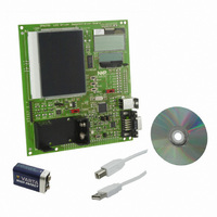
DEMO BOARD LCD GRAPHIC DRIVER
Manufacturer
NXP Semiconductors
Datasheets
1.PCF8576T1118.pdf
(44 pages)
2.OM6290.pdf
(30 pages)
3.OM6290.pdf
(51 pages)
4.OM6290.pdf
(83 pages)
Specifications of OM6290
Main Purpose
Displays, LCD Controller
Embedded
Yes, MCU, 16/32-Bit
Utilized Ic / Part
PCF2119, PCF8531, PCF8576
Primary Attributes
Character, Graphic and Segment LCD Drivers
Secondary Attributes
JTAG, I²C, UART & USB Interfaces
Description/function
Demo Board
Interface Type
USB, I2C, JTAG, UART
Data Bus Width
4 bit, 8 bit, 16 bit
Operating Voltage
1.8 V to 5.5 V
For Use With/related Products
PCF8576DT, PCF2119S, PCF8531
Lead Free Status / RoHS Status
Lead free / RoHS Compliant
Lead Free Status / RoHS Status
Lead free / RoHS Compliant, Lead free / RoHS Compliant
Other names
568-4703


NXP Semiconductors
UM10300_1
User manual
3.1.3 Block diagram
3.2.1 General Description
3.2 Character Driver PCF2119
The PCF2119x is a low power CMOS LCD controller and driver, designed to drive a dot
matrix LCD display of 2-line by 16 or 1-line by 32 characters with 5 x 8 dot format. All
necessary functions for the display are provided in a single chip, including on-chip
temperature compensated generation of LCD bias voltages, resulting in a minimum of
external components and lower system current consumption. The PCF2119x interfaces
to most microcontrollers via a 4 or 8-bit bus or via the 2-wire I
character generator and displays alphanumeric and kana (Japanese) characters. The
letter ‘x’ in PCF2119x characterizes the built-in character set. Various character sets can
be manufactured on request. The character set of the PCF2119 on the demo board is ‘S’.
A similar device is the PCF2113 (2-line by 12 or 1-line by 24 characters + 120 icons).
Fig 2. Block diagram of PCF8576D
SYNC
V
V
OSC
CLK
SDA
V
SCL
LCD
DD
SS
55
54
47
46
49
48
45
44
manufactured in silicon gate CMOS process
AEC-Q100 compliant (TQFP64).
CLOCK SELECT
OSCILLATOR
AND TIMING
FILTERS
INPUT
GENERATOR
LCD BIAS
Rev. 1.0— 8 August 2008
POWER-ON
TIMEBASE
CONTROLLER
BLINKER
RESET
I
2
C-BUS
SA0
SELECTOR
VOLTAGE
53
LCD
BP0
PCF8576DT
COMMAND
DECODER
CONTROLLER
56
BACKPLANE
OUTPUTS
DISPLAY
BP2 BP1 BP3
1
2
3
WRITE DATA
CONTROL
2
DISPLAY SEGMENT OUTPUTS
C-bus. The chip contains a
OUTPUT BANK SELECT
AND BLINK CONTROL
DISPLAY REGISTER
User Manual OM6290
40 × 4-BIT
DISPLAY
S0 to S39
UM10300
RAM
© NXP B.V. 2008. All rights reserved.
4 to 43
DATA POINTER AND
AUTO INCREMENT
SUBADDRESS
A0
COUNTER
50
A1
51
A2
001aab131
10 of 30
52
Related parts for OM6290
Image
Part Number
Description
Manufacturer
Datasheet
Request
R

Part Number:
Description:
NXP Semiconductors designed the LPC2420/2460 microcontroller around a 16-bit/32-bitARM7TDMI-S CPU core with real-time debug interfaces that include both JTAG andembedded trace
Manufacturer:
NXP Semiconductors
Datasheet:

Part Number:
Description:
NXP Semiconductors designed the LPC2458 microcontroller around a 16-bit/32-bitARM7TDMI-S CPU core with real-time debug interfaces that include both JTAG andembedded trace
Manufacturer:
NXP Semiconductors
Datasheet:
Part Number:
Description:
NXP Semiconductors designed the LPC2468 microcontroller around a 16-bit/32-bitARM7TDMI-S CPU core with real-time debug interfaces that include both JTAG andembedded trace
Manufacturer:
NXP Semiconductors
Datasheet:
Part Number:
Description:
NXP Semiconductors designed the LPC2470 microcontroller, powered by theARM7TDMI-S core, to be a highly integrated microcontroller for a wide range ofapplications that require advanced communications and high quality graphic displays
Manufacturer:
NXP Semiconductors
Datasheet:
Part Number:
Description:
NXP Semiconductors designed the LPC2478 microcontroller, powered by theARM7TDMI-S core, to be a highly integrated microcontroller for a wide range ofapplications that require advanced communications and high quality graphic displays
Manufacturer:
NXP Semiconductors
Datasheet:
Part Number:
Description:
The Philips Semiconductors XA (eXtended Architecture) family of 16-bit single-chip microcontrollers is powerful enough to easily handle the requirements of high performance embedded applications, yet inexpensive enough to compete in the market for hi
Manufacturer:
NXP Semiconductors
Datasheet:
Part Number:
Description:
The XA-S3 device is a member of Philips Semiconductors? XA(eXtended Architecture) family of high performance 16-bitsingle-chip microcontrollers
Manufacturer:
NXP Semiconductors
Datasheet:

Part Number:
Description:
The NXP BlueStreak LH75401/LH75411 family consists of two low-cost 16/32-bit System-on-Chip (SoC) devices
Manufacturer:
NXP Semiconductors
Datasheet:
Part Number:
Description:
The NXP LPC3130/3131 combine an 180 MHz ARM926EJ-S CPU core, high-speed USB2
Manufacturer:
NXP Semiconductors
Datasheet:
Part Number:
Description:
The NXP LPC3141 combine a 270 MHz ARM926EJ-S CPU core, High-speed USB 2
Manufacturer:
NXP Semiconductors
Part Number:
Description:
The NXP LPC3143 combine a 270 MHz ARM926EJ-S CPU core, High-speed USB 2
Manufacturer:
NXP Semiconductors

Part Number:
Description:
The NXP LPC3152 combines an 180 MHz ARM926EJ-S CPU core, High-speed USB 2
Manufacturer:
NXP Semiconductors
Part Number:
Description:
The NXP LPC3154 combines an 180 MHz ARM926EJ-S CPU core, High-speed USB 2
Manufacturer:
NXP Semiconductors

Part Number:
Description:
Standard level N-channel enhancement mode Field-Effect Transistor (FET) in a plastic package using NXP High-Performance Automotive (HPA) TrenchMOS technology
Manufacturer:
NXP Semiconductors
Datasheet: