OM6290 NXP Semiconductors, OM6290 Datasheet - Page 5
OM6290
Manufacturer Part Number
OM6290
Description
DEMO BOARD LCD GRAPHIC DRIVER
Manufacturer
NXP Semiconductors
Datasheets
1.PCF8576T1118.pdf
(44 pages)
2.OM6290.pdf
(30 pages)
3.OM6290.pdf
(51 pages)
4.OM6290.pdf
(83 pages)
Specifications of OM6290
Main Purpose
Displays, LCD Controller
Embedded
Yes, MCU, 16/32-Bit
Utilized Ic / Part
PCF2119, PCF8531, PCF8576
Primary Attributes
Character, Graphic and Segment LCD Drivers
Secondary Attributes
JTAG, I²C, UART & USB Interfaces
Description/function
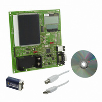
Demo Board
Interface Type
USB, I2C, JTAG, UART
Data Bus Width
4 bit, 8 bit, 16 bit
Operating Voltage
1.8 V to 5.5 V
For Use With/related Products
PCF8576DT, PCF2119S, PCF8531
Lead Free Status / RoHS Status
Lead free / RoHS Compliant
Lead Free Status / RoHS Status
Lead free / RoHS Compliant, Lead free / RoHS Compliant
Other names
568-4703


NXP Semiconductors
UM10300_1
User manual
2.1 Switches
2.2 LED indicators
2.3 Jumpers
For best optical performance, remove the protective foils from the three displays. In order
for the board to work standalone, jumpers J1 and J2 (I
jumper J4. Default position for J4 is ‘Enabled’, enabling LED driver PCA9633 (IC5).
Three switches are present next to the large display LCD3. SW1 is used to select the
predefined patterns/text present in the firmware for display on LCD1. SW2 has the same
function but then for LCD2 and SW3 selects the pattern that will be displayed on LCD3.
Furthermore SW3 can be used to select some lighting modes of backlight BL1 which is
mounted under LCD3.
SW4 is located near the bottom of the board and is the reset switch. At start up all
displays will display some text and when SW1 or SW2 or SW3 is pressed, the displayed
text/pattern on the related display will change.
Switch S1 can be used to select “Program Internal Flash” of the LPC2148 in order to
program modified firmware, or to let the LPC2148 boot from its internal flash.
The OM6290 is a USB-powered device. Alternatively the board can be powered using a
standard 9V (6LR61 / PP3) battery. A battery holder is present on the board and switch
S2, located between the battery holder and LCD3, can be used to select either USB-
power or battery power.
The board contains two LED indicators. LED D7 (green) indicates that +5V is present on
the board, supplied either via USB or via the +9V battery. The +3V3 is derived from +5V.
LED D4 (orange/red, labeled LINK) is on when firmware has been loaded into the flash
memory. If S1 is in position “Program Flash” and the board is reset, D4 goes off and the
board is ready to be flashed. After programming the board, move S1 to “Boot from Flash”
and reset the board by pressing SW4 “RESET”. D4 will turn on now.
The board contains five jumpers.
• J1 (SDA) and J2 (SCL), positioned just below the micro controller, allow
• J3, near the bottom of the board, can usually be left open. If present it allows
• J4 is used to enable/disable the outputs of the PCA9633 LED driver which is used for
• J5 is used to enable the JTAG interface. In this case also connector P4 must be
disconnecting the I
jumpers J1 and J2 are lifted, the I
disconnected and the display drivers can be programmed via any other micro
controller or application with I
GND and 3V3 and 5V are available on the pin strip P3 just above the 9V battery.
resetting the microcontroller via serial interface RS1, required for ISP programming.
backlight BL1. Default position is enabled. If it is put in position ‘uCONTR’ it is
possible to use the firmware to disable and enable the outputs.
mounted on the board. This would be useful to explore the LPC2148 more indepth.
2
Rev. 1.0— 8 August 2008
C bus on the board from the LPC2148 I
2
C-interface. The I
2
C connections to the micro controller are
2
C signals SDA and SCL as well as
2
C) must be placed as well as
2
C interface. When
User Manual OM6290
UM10300
© NXP B.V. 2008. All rights reserved.
5 of 30
Related parts for OM6290
Image
Part Number
Description
Manufacturer
Datasheet
Request
R

Part Number:
Description:
NXP Semiconductors designed the LPC2420/2460 microcontroller around a 16-bit/32-bitARM7TDMI-S CPU core with real-time debug interfaces that include both JTAG andembedded trace
Manufacturer:
NXP Semiconductors
Datasheet:

Part Number:
Description:
NXP Semiconductors designed the LPC2458 microcontroller around a 16-bit/32-bitARM7TDMI-S CPU core with real-time debug interfaces that include both JTAG andembedded trace
Manufacturer:
NXP Semiconductors
Datasheet:
Part Number:
Description:
NXP Semiconductors designed the LPC2468 microcontroller around a 16-bit/32-bitARM7TDMI-S CPU core with real-time debug interfaces that include both JTAG andembedded trace
Manufacturer:
NXP Semiconductors
Datasheet:
Part Number:
Description:
NXP Semiconductors designed the LPC2470 microcontroller, powered by theARM7TDMI-S core, to be a highly integrated microcontroller for a wide range ofapplications that require advanced communications and high quality graphic displays
Manufacturer:
NXP Semiconductors
Datasheet:
Part Number:
Description:
NXP Semiconductors designed the LPC2478 microcontroller, powered by theARM7TDMI-S core, to be a highly integrated microcontroller for a wide range ofapplications that require advanced communications and high quality graphic displays
Manufacturer:
NXP Semiconductors
Datasheet:
Part Number:
Description:
The Philips Semiconductors XA (eXtended Architecture) family of 16-bit single-chip microcontrollers is powerful enough to easily handle the requirements of high performance embedded applications, yet inexpensive enough to compete in the market for hi
Manufacturer:
NXP Semiconductors
Datasheet:
Part Number:
Description:
The XA-S3 device is a member of Philips Semiconductors? XA(eXtended Architecture) family of high performance 16-bitsingle-chip microcontrollers
Manufacturer:
NXP Semiconductors
Datasheet:

Part Number:
Description:
The NXP BlueStreak LH75401/LH75411 family consists of two low-cost 16/32-bit System-on-Chip (SoC) devices
Manufacturer:
NXP Semiconductors
Datasheet:
Part Number:
Description:
The NXP LPC3130/3131 combine an 180 MHz ARM926EJ-S CPU core, high-speed USB2
Manufacturer:
NXP Semiconductors
Datasheet:
Part Number:
Description:
The NXP LPC3141 combine a 270 MHz ARM926EJ-S CPU core, High-speed USB 2
Manufacturer:
NXP Semiconductors
Part Number:
Description:
The NXP LPC3143 combine a 270 MHz ARM926EJ-S CPU core, High-speed USB 2
Manufacturer:
NXP Semiconductors

Part Number:
Description:
The NXP LPC3152 combines an 180 MHz ARM926EJ-S CPU core, High-speed USB 2
Manufacturer:
NXP Semiconductors
Part Number:
Description:
The NXP LPC3154 combines an 180 MHz ARM926EJ-S CPU core, High-speed USB 2
Manufacturer:
NXP Semiconductors

Part Number:
Description:
Standard level N-channel enhancement mode Field-Effect Transistor (FET) in a plastic package using NXP High-Performance Automotive (HPA) TrenchMOS technology
Manufacturer:
NXP Semiconductors
Datasheet: