OM6290 NXP Semiconductors, OM6290 Datasheet - Page 45
OM6290
Manufacturer Part Number
OM6290
Description
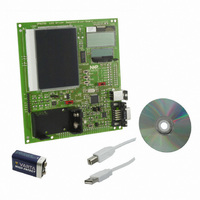
DEMO BOARD LCD GRAPHIC DRIVER
Manufacturer
NXP Semiconductors
Datasheets
1.PCF8576T1118.pdf
(44 pages)
2.OM6290.pdf
(30 pages)
3.OM6290.pdf
(51 pages)
4.OM6290.pdf
(83 pages)
Specifications of OM6290
Main Purpose
Displays, LCD Controller
Embedded
Yes, MCU, 16/32-Bit
Utilized Ic / Part
PCF2119, PCF8531, PCF8576
Primary Attributes
Character, Graphic and Segment LCD Drivers
Secondary Attributes
JTAG, I²C, UART & USB Interfaces
Description/function
Demo Board
Interface Type
USB, I2C, JTAG, UART
Data Bus Width
4 bit, 8 bit, 16 bit
Operating Voltage
1.8 V to 5.5 V
For Use With/related Products
PCF8576DT, PCF2119S, PCF8531
Lead Free Status / RoHS Status
Lead free / RoHS Compliant
Lead Free Status / RoHS Status
Lead free / RoHS Compliant, Lead free / RoHS Compliant
Other names
568-4703


NXP Semiconductors
PCF2119X
Product data sheet
11.2.1 I
11.2.2 I
Two I
PCF2119x.The entire I
Table 33.
Bit 1 of the slave address byte, that a PCF2119x will respond to, is defined by the level
tied to its SA0 input (V
Before any data is transmitted on the I
addressed first. The addressing is always carried out with the first byte transmitted after
the START procedure.
The I
Figure 31
The slow down feature of the I
internal operations) is not used in the PCF2119x.
Definitions:
Bit
2
2
Fig 30. Acknowledgement on the I
•
•
•
•
•
C-bus protocol
C-bus definitions
Transmitter: the device which sends the data to the bus.
Receiver: the device which receives the data from the bus.
Master: the device which initiates a transfer, generates clock signals and terminates a
transfer.
Slave: the device addressed by a master.
Multi-master: more than one master can attempt to control the bus at the same time
without corrupting the message.
2
2
C-bus configuration for the different PCF2119x read and write cycles is shown in
C-bus slave addresses (0111 010 and 0111 011) are reserved for the
by transmitter
data output
by receiver
data output
SCL from
to
Slave address
7
MSB
0
I
2
master
C slave address byte
Figure
All information provided in this document is subject to legal disclaimers.
33.
condition
6
1
START
SS
2
S
C-bus slave address byte is shown in
Rev. 9 — 14 April 2011
for logic 0 and V
5
1
2
C-bus protocol (receiver holds SCL line LOW during
1
2
C-bus
2
C-bus, the device which should respond is
4
1
DD
for logic 1).
2
3
0
not acknowledge
2
1
acknowledge
Table
8
LCD controllers/drivers
33.
PCF2119x
acknowledgement
clock pulse for
1
SA0
© NXP B.V. 2011. All rights reserved.
9
mbc602
0
LSB
R/W
45 of 83
Related parts for OM6290
Image
Part Number
Description
Manufacturer
Datasheet
Request
R

Part Number:
Description:
NXP Semiconductors designed the LPC2420/2460 microcontroller around a 16-bit/32-bitARM7TDMI-S CPU core with real-time debug interfaces that include both JTAG andembedded trace
Manufacturer:
NXP Semiconductors
Datasheet:

Part Number:
Description:
NXP Semiconductors designed the LPC2458 microcontroller around a 16-bit/32-bitARM7TDMI-S CPU core with real-time debug interfaces that include both JTAG andembedded trace
Manufacturer:
NXP Semiconductors
Datasheet:
Part Number:
Description:
NXP Semiconductors designed the LPC2468 microcontroller around a 16-bit/32-bitARM7TDMI-S CPU core with real-time debug interfaces that include both JTAG andembedded trace
Manufacturer:
NXP Semiconductors
Datasheet:
Part Number:
Description:
NXP Semiconductors designed the LPC2470 microcontroller, powered by theARM7TDMI-S core, to be a highly integrated microcontroller for a wide range ofapplications that require advanced communications and high quality graphic displays
Manufacturer:
NXP Semiconductors
Datasheet:
Part Number:
Description:
NXP Semiconductors designed the LPC2478 microcontroller, powered by theARM7TDMI-S core, to be a highly integrated microcontroller for a wide range ofapplications that require advanced communications and high quality graphic displays
Manufacturer:
NXP Semiconductors
Datasheet:
Part Number:
Description:
The Philips Semiconductors XA (eXtended Architecture) family of 16-bit single-chip microcontrollers is powerful enough to easily handle the requirements of high performance embedded applications, yet inexpensive enough to compete in the market for hi
Manufacturer:
NXP Semiconductors
Datasheet:
Part Number:
Description:
The XA-S3 device is a member of Philips Semiconductors? XA(eXtended Architecture) family of high performance 16-bitsingle-chip microcontrollers
Manufacturer:
NXP Semiconductors
Datasheet:

Part Number:
Description:
The NXP BlueStreak LH75401/LH75411 family consists of two low-cost 16/32-bit System-on-Chip (SoC) devices
Manufacturer:
NXP Semiconductors
Datasheet:
Part Number:
Description:
The NXP LPC3130/3131 combine an 180 MHz ARM926EJ-S CPU core, high-speed USB2
Manufacturer:
NXP Semiconductors
Datasheet:
Part Number:
Description:
The NXP LPC3141 combine a 270 MHz ARM926EJ-S CPU core, High-speed USB 2
Manufacturer:
NXP Semiconductors
Part Number:
Description:
The NXP LPC3143 combine a 270 MHz ARM926EJ-S CPU core, High-speed USB 2
Manufacturer:
NXP Semiconductors

Part Number:
Description:
The NXP LPC3152 combines an 180 MHz ARM926EJ-S CPU core, High-speed USB 2
Manufacturer:
NXP Semiconductors
Part Number:
Description:
The NXP LPC3154 combines an 180 MHz ARM926EJ-S CPU core, High-speed USB 2
Manufacturer:
NXP Semiconductors

Part Number:
Description:
Standard level N-channel enhancement mode Field-Effect Transistor (FET) in a plastic package using NXP High-Performance Automotive (HPA) TrenchMOS technology
Manufacturer:
NXP Semiconductors
Datasheet: