OM6290 NXP Semiconductors, OM6290 Datasheet - Page 52
OM6290
Manufacturer Part Number
OM6290
Description
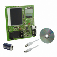
DEMO BOARD LCD GRAPHIC DRIVER
Manufacturer
NXP Semiconductors
Datasheets
1.PCF8576T1118.pdf
(44 pages)
2.OM6290.pdf
(30 pages)
3.OM6290.pdf
(51 pages)
4.OM6290.pdf
(83 pages)
Specifications of OM6290
Main Purpose
Displays, LCD Controller
Embedded
Yes, MCU, 16/32-Bit
Utilized Ic / Part
PCF2119, PCF8531, PCF8576
Primary Attributes
Character, Graphic and Segment LCD Drivers
Secondary Attributes
JTAG, I²C, UART & USB Interfaces
Description/function
Demo Board
Interface Type
USB, I2C, JTAG, UART
Data Bus Width
4 bit, 8 bit, 16 bit
Operating Voltage
1.8 V to 5.5 V
For Use With/related Products
PCF8576DT, PCF2119S, PCF8531
Lead Free Status / RoHS Status
Lead free / RoHS Compliant
Lead Free Status / RoHS Status
Lead free / RoHS Compliant, Lead free / RoHS Compliant
Other names
568-4703


NXP Semiconductors
15. Dynamic characteristics
Table 37.
V
otherwise specified.
PCF2119X
Product data sheet
Symbol
Clock and oscillator
f
f
f
t
Timing characteristics of parallel interface
Write operation (writing data from microcontroller to PCF2119x); see
t
t
t
t
t
t
Read operation (reading data from PCF2119x to microcontroller); see
t
t
t
t
t
t
Timing characteristics of I
f
t
t
t
t
t
t
C
t
t
fr(LCD)
osc
osc(ext)
d(startup)(OSC)
cy(en)
w(en)
su(A)
h(A)
su(D)
h(D)
cy(en)
w(en)
su(A)
h(A)
d(DV)
h(D)
SCL
LOW
HIGH
SU;DAT
HD;DAT
r
f
SU;STA
HD;STA
DD1
b
= 1.5 V to 5.5 V; V
Dynamic characteristics
Parameter
LCD frame frequency
oscillator frequency
external oscillator frequency
start-up delay time on pin OSC oscillator, after power-down
enable cycle time
enable pulse width
address set-up time
address hold time
data input set-up time
data input hold time
enable cycle time
enable pulse width
address set-up time
address hold time
data input valid delay time
data input hold time
SCL clock frequency
LOW period of the SCL clock
HIGH period of the SCL clock
data set-up time
data hold time
rise time of both SDA and SCL
signals
fall time of both SDA and SCL
signals
capacitive load for each bus
line
set-up time for a repeated
START condition
hold time (repeated) START
condition
DD2
= V
2
C-bus interface
DD3
= 2.2 V to 4.0 V; V
All information provided in this document is subject to legal disclaimers.
[2]
[2]
; see
Conditions
internal clock; V
not available at any pin
V
V
DD1
DD1
Rev. 9 — 14 April 2011
SS
Figure 36
> 2.2 V
> 1.5 V
= 0 V; V
LCD
DD
= 5.0 V
= 2.2 V to 6.5 V; T
Figure 34
Figure 35
[1][3]
[1][3]
[1]
140
140
60
-
1.3
Min
45
-
500
220
50
25
25
500
220
50
25
-
-
20
0.6
100
0
15 + 0.1 C
15 + 0.1 C
-
0.6
0.6
amb
=
−
40
b
b
LCD controllers/drivers
°
C to +85
Typ
95
250
-
200
-
-
-
-
-
-
-
-
-
-
-
-
-
-
-
-
-
-
-
-
-
-
-
PCF2119x
© NXP B.V. 2011. All rights reserved.
°
Max
147
450
450
300
-
-
-
-
-
-
-
-
-
-
150
250
100
400
-
-
-
-
300
300
400
-
-
C; unless
kHz
kHz
ns
kHz
Unit
Hz
μs
ns
ns
ns
ns
ns
ns
ns
ns
ns
ns
ns
ns
μs
μs
ns
ns
ns
ns
pF
μs
μs
52 of 83
Related parts for OM6290
Image
Part Number
Description
Manufacturer
Datasheet
Request
R

Part Number:
Description:
NXP Semiconductors designed the LPC2420/2460 microcontroller around a 16-bit/32-bitARM7TDMI-S CPU core with real-time debug interfaces that include both JTAG andembedded trace
Manufacturer:
NXP Semiconductors
Datasheet:

Part Number:
Description:
NXP Semiconductors designed the LPC2458 microcontroller around a 16-bit/32-bitARM7TDMI-S CPU core with real-time debug interfaces that include both JTAG andembedded trace
Manufacturer:
NXP Semiconductors
Datasheet:
Part Number:
Description:
NXP Semiconductors designed the LPC2468 microcontroller around a 16-bit/32-bitARM7TDMI-S CPU core with real-time debug interfaces that include both JTAG andembedded trace
Manufacturer:
NXP Semiconductors
Datasheet:
Part Number:
Description:
NXP Semiconductors designed the LPC2470 microcontroller, powered by theARM7TDMI-S core, to be a highly integrated microcontroller for a wide range ofapplications that require advanced communications and high quality graphic displays
Manufacturer:
NXP Semiconductors
Datasheet:
Part Number:
Description:
NXP Semiconductors designed the LPC2478 microcontroller, powered by theARM7TDMI-S core, to be a highly integrated microcontroller for a wide range ofapplications that require advanced communications and high quality graphic displays
Manufacturer:
NXP Semiconductors
Datasheet:
Part Number:
Description:
The Philips Semiconductors XA (eXtended Architecture) family of 16-bit single-chip microcontrollers is powerful enough to easily handle the requirements of high performance embedded applications, yet inexpensive enough to compete in the market for hi
Manufacturer:
NXP Semiconductors
Datasheet:
Part Number:
Description:
The XA-S3 device is a member of Philips Semiconductors? XA(eXtended Architecture) family of high performance 16-bitsingle-chip microcontrollers
Manufacturer:
NXP Semiconductors
Datasheet:

Part Number:
Description:
The NXP BlueStreak LH75401/LH75411 family consists of two low-cost 16/32-bit System-on-Chip (SoC) devices
Manufacturer:
NXP Semiconductors
Datasheet:
Part Number:
Description:
The NXP LPC3130/3131 combine an 180 MHz ARM926EJ-S CPU core, high-speed USB2
Manufacturer:
NXP Semiconductors
Datasheet:
Part Number:
Description:
The NXP LPC3141 combine a 270 MHz ARM926EJ-S CPU core, High-speed USB 2
Manufacturer:
NXP Semiconductors
Part Number:
Description:
The NXP LPC3143 combine a 270 MHz ARM926EJ-S CPU core, High-speed USB 2
Manufacturer:
NXP Semiconductors

Part Number:
Description:
The NXP LPC3152 combines an 180 MHz ARM926EJ-S CPU core, High-speed USB 2
Manufacturer:
NXP Semiconductors
Part Number:
Description:
The NXP LPC3154 combines an 180 MHz ARM926EJ-S CPU core, High-speed USB 2
Manufacturer:
NXP Semiconductors

Part Number:
Description:
Standard level N-channel enhancement mode Field-Effect Transistor (FET) in a plastic package using NXP High-Performance Automotive (HPA) TrenchMOS technology
Manufacturer:
NXP Semiconductors
Datasheet: