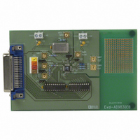
EVAL-AD9830EBZ Analog Devices Inc, EVAL-AD9830EBZ Datasheet - Page 2
EVAL-AD9830EBZ
Manufacturer Part Number
EVAL-AD9830EBZ
Description
BOARD EVALUATION AD9830
Manufacturer
Analog Devices Inc
Specifications of EVAL-AD9830EBZ
Main Purpose
Timing, Direct Digital Synthesis (DDS)
Utilized Ic / Part
AD9830
Lead Free Status / RoHS Status
Lead free / RoHS Compliant
Secondary Attributes
-
Embedded
-
Primary Attributes
-
Lead Free Status / Rohs Status
Supplier Unconfirmed


NOTES
1
2
3
4
5
The AD9830 is tested with a capacitive load of 50 pF. The part can be operated
with higher capacitive loads, but the magnitude of the analog output will be attenu-
ated. For example, a 10 MHz output signal will be attenuated by 3 dB when the
load capacitance equals 250 pF.
Specifications subject to change without notice.
Parameter
SIGNAL DAC SPECIFICATIONS
DDS SPECIFICATIONS
VOLTAGE REFERENCE
LOGIC INPUTS
POWER SUPPLIES
AD9830–SPECIFICATIONS
Operating temperature range is as follows: A Version: –40 C to +85 C.
All dynamic specifications are measured using IOUT. 100% production tested.
f
Measured with the digital inputs static and equal to 0 V or DVDD.
The Low Power Sleep Mode current is 2 mA typically when a 1 M
not tied from REFOUT to AGND.
MCLK
Resolution
Update Rate (f
I
Output Compliance
DC Accuracy
Dynamic Specifications
Clock Feedthrough
Wake Up Time
Power-Down Option
Internal Reference @ +25 C
REFIN Input Impedance
Reference TC
REFOUT Impedance
V
V
I
C
AVDD
DVDD
I
I
I
Low Power Sleep Mode
OUT
INH
AA
DD
AA
INH
INL
IN
Integral Nonlinearity
Differential Nonlinearity
Signal-to-Noise Ratio
Total Harmonic Distortion
Spurious Free Dynamic Range (SFDR)
T
= 6.25 MHz, Frequency Word = 5671C71C HEX, f
, Input Capacitance
+ I
MIN
, Input Current
Narrow Band
Wide Band ( 2 MHz)
, Input Low Voltage
, Input High Voltage
Full Scale
( 50 kHz)
( 200 kHz)
DD
to T
4
MAX
MAX
)
2
5
3
OUT
= 2.11 MHz.
AD9830A
10
50
20
1
50
–53
–72
–68
–50
–55
1
Yes
1.21
1.21
10
100
300
V
0.9
10
10
4.75/5.25
4.75/5.25
25
6 + 0.5/MHz
60
0.25
1
1
1
0.5
DD
(V
R
resistor is
SET
–0.9
DD
= 1 k ; R
= +5 V
7%
–2–
LOAD
5%; AGND = DGND = 0 V; T
10nF
= 51
Figure 1. Test Circuit with Which Specifications Are
Tested
Units
Bits
MSPS max
mA max
V max
LSB typ
LSB typ
dB min
dBc max
dBc min
dBc min
dBc min
dBc typ
ms typ
Volts typ
Volts min/max
M typ
ppm/ C typ
V min
V max
pF max
V min/V max
V min/V max
mA max
mA typ
mA max
mA typ
mA max
A max
12
REFOUT
typ
REFERENCE
ON-BOARD
for IOUT and IOUT unless otherwise noted)
ROM
SIN
REFIN
FULL-SCALE
CONTROL
A
10-BIT
Test Conditions/Comments
f
f
f
f
1 M Resistor Tied Between
REFOUT and AGND
= T
ADJUST
DAC
MCLK
MCLK
MCLK
OUT
FS
MIN
= 2 MHz
= f
= f
= 6.25 MHz, f
to T
MAX
MAX
COMP
MAX
IOUT
IOUT
; REFIN = REFOUT;
, f
, f
OUT
OUT
51
R
1k
SET
AVDD
= 2 MHz
= 2 MHz
OUT
10nF
50pF
= 2.11 MHz
51
REV. A
50pF
Related parts for EVAL-AD9830EBZ
Image
Part Number
Description
Manufacturer
Datasheet
Request
R


Part Number:
Description:
BOARD EVAL FOR SI270X-A
Manufacturer:
Silicon Laboratories Inc
Datasheet:

Part Number:
Description:
BUCK CONV REF DESIGN KIT IP1201
Manufacturer:
International Rectifier
Datasheet:
Part Number:
Description:
BOARD DEMO SYNC DUAL BUCK CNVTER
Manufacturer:
International Rectifier
Datasheet:
Part Number:
Description:
BOARD DEMO SYNC BUCK CONVETER
Manufacturer:
International Rectifier
Datasheet:

Part Number:
Description:
EVALBOARD/EB Omnidirectional microphone - Analog
Manufacturer:
Analog Devices
Datasheet:
Part Number:
Description:
EVALBOARD/EB Omnidirectional microphone - Analog
Manufacturer:
Analog Devices
Datasheet:


Part Number:
Description:
BOARD EVAL LED DRIVER LT3756
Manufacturer:
Linear Technology
Datasheet:

Part Number:
Description:
BOARD EVAL FOR AD7741/7742
Manufacturer:
Analog Devices Inc
Datasheet:

Part Number:
Description:
±1.7g Dual-Axis IMEMS Accelerometer Evaluation Board
Manufacturer:
Analog Devices Inc
Datasheet:

Part Number:
Description:
IC MULTIPLIER ANALOG 8-SOIC T/R
Manufacturer:
Analog Devices Inc
Datasheet:

Part Number:
Description:
IC ANALOG MULTIPLIER 8-DIP
Manufacturer:
Analog Devices Inc
Datasheet:
Part Number:
Description:
IC ANALOG MULTIPLIER 8-SOIC
Manufacturer:
Analog Devices Inc
Datasheet:
Part Number:
Description:
IC ANALOG MULTIPLIER 8-DIP
Manufacturer:
Analog Devices Inc
Datasheet: