CDB5376 Cirrus Logic Inc, CDB5376 Datasheet - Page 21
CDB5376
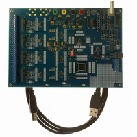
Manufacturer Part Number
CDB5376
Description
EVALUATION BOARD FOR CS5376
Manufacturer
Cirrus Logic Inc
Datasheets
1.CS5371A-ISZR.pdf
(32 pages)
2.CS4373A-ISZ.pdf
(34 pages)
3.CS5376A-IQZR.pdf
(106 pages)
4.CDB5378.pdf
(16 pages)
5.CDB5376.pdf
(80 pages)
6.CDB5376.pdf
(16 pages)
Specifications of CDB5376
Main Purpose
Seismic Evaluation System
Embedded
Yes, MCU, 8-Bit
Utilized Ic / Part
CS3301A, CS3302A, CS4373A, CS5372A, CS5376A
Primary Attributes
Quad Digital Filter
Secondary Attributes
Graphical User Interface, SPI™ & USB Interfaces
Processor To Be Evaluated
CS330x, CS4373A, CS537x
Interface Type
USB
Lead Free Status / RoHS Status
Contains lead / RoHS non-compliant
Lead Free Status / RoHS Status
Lead free / RoHS Compliant, Contains lead / RoHS non-compliant
Other names
598-1778


7. VOLTAGE REFERENCE
The CS5371A and CS5372A modulators re-
quire a 2.500 V precision voltage reference to
be supplied to the VREF
7.1 VREF Power Supply
To guarantee proper regulation headroom for
the voltage reference device, the voltage refer-
ence GND pin should be connected to VA- in-
stead of system ground, as shown in
Figure
voltage equal to VA- and a VREF+ voltage
very near ground [(VA-) + 2.500 VREF].
Power supply inputs to the voltage reference
device should be bypassed to system ground
with 0.1 μF capacitors placed as close as pos-
sible to the power and ground pins. In addition
to 0.1 μF local bypass capacitors, at least
100 μF of bulk capacitance to system ground
should be placed on each power supply near
the voltage regulator outputs. Bypass capaci-
tors should be X7R, C0G, tantalum, or other
high-quality dielectric type.
7.2 VREF RC Filter
A primary concern in selecting a precision volt-
age reference device is noise performance in
the measurement bandwidth. The
Technology LT1019AIS8-2.5
ence yields acceptable noise levels if the out-
put is filtered with a low-pass RC filter.
A separate RC filter is required for each sys-
tem device connected to a given voltage refer-
DS748F3
14. This connection results in a VREF-
From VA+
Regulator
From VA-
Regulator
100 μF
100 μF
±
pins.
Figure 14. Voltage Reference Circuit
voltage refer-
0.1 μF
0.1 μF
2.500 V
Linear
VREF
10 Ω
ence output. By sharing a common RC filter,
signal-dependent sampling of the voltage ref-
erence by one system device could cause un-
wanted tones to appear in the measurement
bandwidth of another system device via com-
mon impedance coupling.
7.3 VREF PCB Routing
To minimize the possibility of outside noise
coupling into the CS5371A and CS5372A volt-
age reference input, the VREF
be routed as a differential pair from the large
capacitor of the voltage reference RC filter.
Careful control of the voltage reference source
and return currents by routing VREF
ferential pair will significantly improve immuni-
ty from external noise.
To further improve noise rejection of the
VREF
pass
possible to the VREF+ and VREF- pins of the
CS5371A and CS5372A.
7.4 VREF Input Impedance
The switched-capacitor input architecture of
the VREF
ance that depends on the internal capacitor
size and the MCLK frequency. With a 15 pF in-
ternal capacitor and a 2.048 MHz MCLK, the
VREF input impedance is approximately
1 / [(2.048 MHz) x (15 pF)] = 32 kΩ. While the
size of the internal capacitor is fixed, the volt-
0.1 μF
capacitors to system ground as close as
± differential route,
±
+
Route VREF
from the 100uF RC filter capacitor
100 μF
inputs results in an input imped-
CS5371A CS5372A
±
as a differential pair
0.1 μF
0.1 μF
include 0.1 μF
To VREF+
To VREF-
±
traces should
±
as a dif-
by-
21
Related parts for CDB5376
Image
Part Number
Description
Manufacturer
Datasheet
Request
R

Part Number:
Description:
Development Kit
Manufacturer:
Cirrus Logic Inc
Datasheet:
Part Number:
Description:
Development Kit
Manufacturer:
Cirrus Logic Inc
Datasheet:


Part Number:
Description:
High-efficiency PFC + Fluorescent Lamp Driver Reference Design
Manufacturer:
Cirrus Logic Inc
Datasheet:
Part Number:
Description:
Development Kit
Manufacturer:
Cirrus Logic Inc
Datasheet:
Part Number:
Description:
Development Kit
Manufacturer:
Cirrus Logic Inc
Datasheet:

Part Number:
Description:
Development Kit
Manufacturer:
Cirrus Logic Inc
Datasheet:
Part Number:
Description:
Development Kit
Manufacturer:
Cirrus Logic Inc
Datasheet:
Part Number:
Description:
Development Kit
Manufacturer:
Cirrus Logic Inc
Datasheet:
Part Number:
Description:
Development Kit
Manufacturer:
Cirrus Logic Inc
Datasheet:

Part Number:
Description:
EVALUATION BOARD FOR CS8427
Manufacturer:
Cirrus Logic Inc
Datasheet:

Part Number:
Description:
BOARD EVAL FOR CS8416 RCVR
Manufacturer:
Cirrus Logic Inc
Datasheet:

Part Number:
Description:
EVALUATION BOARD FOR CS8420
Manufacturer:
Cirrus Logic Inc
Datasheet:

Part Number:
Description:
KIT DEVELOPMENT EP9315 ARM9
Manufacturer:
Cirrus Logic Inc
Datasheet:

Part Number:
Description:
KIT DEVELOPMENT EP9302 ARM9
Manufacturer:
Cirrus Logic Inc
Datasheet: