CDB5376 Cirrus Logic Inc, CDB5376 Datasheet - Page 26
CDB5376
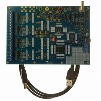
Manufacturer Part Number
CDB5376
Description
EVALUATION BOARD FOR CS5376
Manufacturer
Cirrus Logic Inc
Datasheets
1.CS5371A-ISZR.pdf
(32 pages)
2.CS4373A-ISZ.pdf
(34 pages)
3.CS5376A-IQZR.pdf
(106 pages)
4.CDB5378.pdf
(16 pages)
5.CDB5376.pdf
(80 pages)
6.CDB5376.pdf
(16 pages)
Specifications of CDB5376
Main Purpose
Seismic Evaluation System
Embedded
Yes, MCU, 8-Bit
Utilized Ic / Part
CS3301A, CS3302A, CS4373A, CS5372A, CS5376A
Primary Attributes
Quad Digital Filter
Secondary Attributes
Graphical User Interface, SPI™ & USB Interfaces
Processor To Be Evaluated
CS330x, CS4373A, CS537x
Interface Type
USB
Lead Free Status / RoHS Status
Contains lead / RoHS non-compliant
Lead Free Status / RoHS Status
Lead free / RoHS Compliant, Contains lead / RoHS non-compliant
Other names
598-1778


VREF+
VREF-
Digital Inputs
MCLK
MSYNC
OFST
PWDN
Digital Outputs
MDATA
MFLAG
26
Input for an external +2.500 V voltage reference relative to VREF-.
This pin should be tied to VA- near the voltage reference output.
A CMOS compatible clock input for the modulator internal master clock, nominally 2.048 MHz
with an amplitude equal to the VD digital power supply.
A low to high transition resets the internal clock phasing of the modulator. This assures the
sampling instant and modulator data output are synchronous to the external system.
_
When high, adds approximately -60 mV or -35 mV of internal differential offset to the analog
input signal to guarantee any ΔΣ idle tones are removed. When low, no offset is added.
When high, the modulator is in power-down mode. Halting MCLK while in power down mode
reduces modulator power dissipation further.
Modulator data is output as a 1-bit serial data stream at 512 kHz with an MCLK input of
2.048 MHz.
A high level output indicates the modulator is unstable due to an over-range on the analog
inputs.
_
_
_
_
Offset Mode Select, pin 14
_
_
_
Modulator Clock Input, pin 19
Negative Voltage Reference Input, pin 6
Power-down Mode, pin 24
Positive Voltage Reference Input, pin 5
Modulator Data Output, pin 21
Modulator Flag Output, pin 22
Modulator Sync Input, pin 20
CS5371A CS5372A
DS748F3
Related parts for CDB5376
Image
Part Number
Description
Manufacturer
Datasheet
Request
R

Part Number:
Description:
Development Kit
Manufacturer:
Cirrus Logic Inc
Datasheet:
Part Number:
Description:
Development Kit
Manufacturer:
Cirrus Logic Inc
Datasheet:


Part Number:
Description:
High-efficiency PFC + Fluorescent Lamp Driver Reference Design
Manufacturer:
Cirrus Logic Inc
Datasheet:
Part Number:
Description:
Development Kit
Manufacturer:
Cirrus Logic Inc
Datasheet:
Part Number:
Description:
Development Kit
Manufacturer:
Cirrus Logic Inc
Datasheet:

Part Number:
Description:
Development Kit
Manufacturer:
Cirrus Logic Inc
Datasheet:
Part Number:
Description:
Development Kit
Manufacturer:
Cirrus Logic Inc
Datasheet:
Part Number:
Description:
Development Kit
Manufacturer:
Cirrus Logic Inc
Datasheet:
Part Number:
Description:
Development Kit
Manufacturer:
Cirrus Logic Inc
Datasheet:

Part Number:
Description:
EVALUATION BOARD FOR CS8427
Manufacturer:
Cirrus Logic Inc
Datasheet:

Part Number:
Description:
BOARD EVAL FOR CS8416 RCVR
Manufacturer:
Cirrus Logic Inc
Datasheet:

Part Number:
Description:
EVALUATION BOARD FOR CS8420
Manufacturer:
Cirrus Logic Inc
Datasheet:

Part Number:
Description:
KIT DEVELOPMENT EP9315 ARM9
Manufacturer:
Cirrus Logic Inc
Datasheet:

Part Number:
Description:
KIT DEVELOPMENT EP9302 ARM9
Manufacturer:
Cirrus Logic Inc
Datasheet: