CP2201EK Silicon Laboratories Inc, CP2201EK Datasheet - Page 73
CP2201EK
Manufacturer Part Number
CP2201EK
Description
KIT EVAL FOR CP2201 ETH CTRLR
Manufacturer
Silicon Laboratories Inc
Type
Controllers & Processorsr
Specifications of CP2201EK
Main Purpose
Interface, Ethernet Sensor
Embedded
Yes, MCU, 8-Bit
Utilized Ic / Part
CP2200, CP2201
Primary Attributes
Temperature and Light Sensor
Secondary Attributes
Graphic User Interface
Interface Type
Ethernet
Product
Modules
Silicon Manufacturer
Silicon Labs
Silicon Core Number
CP2201
Silicon Family Name
CP220x
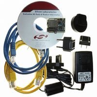
Kit Contents
CP2201 Evaluation Board, Power Adapter, CAT5e Ethernet Cable, CD-ROM, Quick-Start Guide
For Use With/related Products
CP2201
Lead Free Status / RoHS Status
Contains lead / RoHS non-compliant
Lead Free Status / RoHS Status
Lead free / RoHS Compliant, Contains lead / RoHS non-compliant
Other names
336-1316
Available stocks
Company
Part Number
Manufacturer
Quantity
Price
Company:

Part Number:
CP2201EK
Manufacturer:
SiliconL
Quantity:
8


13. Flash Memory
The CP2200/1 has 8 kB of on-chip non-volatile Flash memory fully accessible by the host processor. The last six
bytes of this memory space (addresses 0x1FFA to 0x1FFF) are factory preprogrammed and contain a unique 48-
bit MAC Address (Individual Address) registered with the IEEE Registration Authority. The most significant byte of
the MAC address is at 0x1FFA, and the least significant byte is at 0x1FFF. The last page of Flash containing the
MAC address is erasable, and the user should exercise caution to prevent erasing the MAC Address.
13.1. Programming the Flash Memory
The Flash memory can be programmed one byte at a time through the parallel host interface. Once cleared to a
logic 0, a Flash bit must be erased to set it back to logic 1. A Flash bit may always be changed from logic 1 to
logic 0, as long as Flash bytes are only written once between erase cycles. Flash erase operations erase an entire
512 byte sector at a time. Flash write and erase operations are automatically timed by hardware and do not affect
the parallel host interface. After initiating a Flash write or erase operation, the host CPU can continue to access the
CP2200/1 through the parallel host interface while the Flash operation is taking place. The host is notified with an
interrupt request when the Flash write or erase operation is complete. Refer to Table 18 for complete Flash
memory electrical characteristics including typical write and erase cycle times.
The Flash memory can be written and erased using the FLASHADDRH:FLASHADDRL, FLASHDATA, and
FLASHERASE registers. Once a Flash operation is initiated, the status can be monitored using the FLASHSTA
register, or the host can wait for notification by the interrupt signal.
13.1.1. Flash Lock and Key Protection
The Flash memory is protected from errant write and erase operations by a lock and key function. Flash reads are
unrestricted. The Flash Lock and Key Register (FLASHKEY) must be written with the correct key codes, in
sequence, before each Flash write or erase operation. If a Flash write or erase operation is attempted without first
writing the correct key codes to the FLASHKEY register, Flash cannot be written or erased until the next reset.
After programming Flash, the CP2200/1 should be reset in order to protect the device from errant Flash operations.
The key codes for unlocking the CP2200/1 are 0xA5 and 0xF1. These codes must be written in sequence to the
FLASHKEY register prior to each Flash write or erase operation. Note: To ensure the integrity of Flash
contents, the on-chip V
13.1.2. Flash Erase Procedure
13.1.3. Flash Write Procedure
Step 1: Write 0xA5 followed by 0xF1 to FLASHKEY.
Step 2: Set FLASHADDRH:FLASHADDRL to any address within the 512-byte page to be erased.
Step 3: Write the value 0x01 to FLASHERASE.
Step 4: Check FLASHSTA to determine when the Flash operation is complete. The Flash Write/Erase
Step 1: Write 0xA5 followed by 0xF1 to FLASHKEY.
Step 2: If the byte to be written is not 0xFF, then erase the page containing the byte.
Step 3: Set FLASHADDRH:FLASHADDRL to the address of the byte to be written.
Step 4: Write the value to be written to the FLASHDATA register.
Step 5: Check FLASHSTA to determine when the Flash operation is complete. The Flash Write/Erase
Completed interrupt can also be use to determine when the operation completes.
Completed interrupt can also be used to determine when the operation is complete.
DD
Monitor should not be disabled while the Flash memory is unlocked.
Rev. 1.0
CP2200/1
73
Related parts for CP2201EK
Image
Part Number
Description
Manufacturer
Datasheet
Request
R

Part Number:
Description:
IC ETH CTRLR SNGL-CHIP 28QFN
Manufacturer:
Silicon Laboratories Inc
Datasheet:

Part Number:
Description:
Ethernet ICs Ethernet Controller
Manufacturer:
Silicon Laboratories Inc

Part Number:
Description:
SMD/C°/SINGLE-ENDED OUTPUT SILICON OSCILLATOR
Manufacturer:
Silicon Laboratories Inc
Part Number:
Description:
Manufacturer:
Silicon Laboratories Inc
Datasheet:
Part Number:
Description:
N/A N/A/SI4010 AES KEYFOB DEMO WITH LCD RX
Manufacturer:
Silicon Laboratories Inc
Datasheet:
Part Number:
Description:
N/A N/A/SI4010 SIMPLIFIED KEY FOB DEMO WITH LED RX
Manufacturer:
Silicon Laboratories Inc
Datasheet:
Part Number:
Description:
N/A/-40 TO 85 OC/EZLINK MODULE; F930/4432 HIGH BAND (REV E/B1)
Manufacturer:
Silicon Laboratories Inc
Part Number:
Description:
EZLink Module; F930/4432 Low Band (rev e/B1)
Manufacturer:
Silicon Laboratories Inc
Part Number:
Description:
I°/4460 10 DBM RADIO TEST CARD 434 MHZ
Manufacturer:
Silicon Laboratories Inc
Part Number:
Description:
I°/4461 14 DBM RADIO TEST CARD 868 MHZ
Manufacturer:
Silicon Laboratories Inc
Part Number:
Description:
I°/4463 20 DBM RFSWITCH RADIO TEST CARD 460 MHZ
Manufacturer:
Silicon Laboratories Inc
Part Number:
Description:
I°/4463 20 DBM RADIO TEST CARD 868 MHZ
Manufacturer:
Silicon Laboratories Inc
Part Number:
Description:
I°/4463 27 DBM RADIO TEST CARD 868 MHZ
Manufacturer:
Silicon Laboratories Inc
Part Number:
Description:
I°/4463 SKYWORKS 30 DBM RADIO TEST CARD 915 MHZ
Manufacturer:
Silicon Laboratories Inc