KIT33887EKEVBE Freescale Semiconductor, KIT33887EKEVBE Datasheet - Page 4
KIT33887EKEVBE
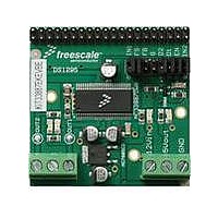
Manufacturer Part Number
KIT33887EKEVBE
Description
BOARD EVALUATION FOR MC33887
Manufacturer
Freescale Semiconductor
Type
Charge Pumpsr
Specifications of KIT33887EKEVBE
Main Purpose
Power Management, H Bridge Driver (Internal FET)
Embedded
No
Utilized Ic / Part
MC33887
Primary Attributes
5A, 5 ~ 28V, PWM to 20kHz, Active Current Limit
Secondary Attributes
Fault Status, Sleep Mode, Proportional Current Mirror Output
Input Voltage
8 V to 20 V
Board Size
50.8 mm x 50.8 mm
Maximum Operating Temperature
+ 85 C
Product
Power Management Modules
Dimensions
50.8 mm x 50.8 mm
Silicon Manufacturer
Freescale
Silicon Core Number
MC33887
Kit Application Type
Power Management - Motor Control
Application Sub Type
DC Brushed Motor
Kit Contents
Board, CD
Rohs Compliant
Yes
Lead Free Status / RoHS Status
Lead free / RoHS Compliant
For Use With/related Products
MC33887


4
Table 2. PQFN PIN DEFINITIONS
33887
PIN CONNECTIONS
Transparent Top View of Package
5, 6, 12, 13, 34, 35
A functional description of each pin can be found in the
14, 15, 17, 18
29, 30, 32, 33
1, 7, 10, 16,
19, 28, 31
21– 26
Pad
Pin
11
20
27
36
2
3
4
8
9
Pin Name
Interface
Thermal
AGND
PGND
OUT1
OUT2
CCP
NC
IN2
IN1
D1
EN
FS
FB
D2
V+
Fault Status for H-Bridge
Charge Pump Capacitor
Feedback for H-Bridge
Positive Power Supply
Exposed Pad Thermal
Logic Input Control 2
Logic Input Control 1
H-Bridge Output 1
H-Bridge Output 2
AGND
Analog Ground
Power Ground
Formal Name
No Connect
IN2
NC
NC
NC
EN
D1
FS
V+
V+
Disable 1
Disable 2
Interface
Enable
Figure 4. 33887 Pin Connections
10
1
2
3
4
5
6
7
8
9
Functional Pin DescriptionS
No internal connection to this pin.
Active HIGH input used to simultaneously tri-state disable both H-Bridge
outputs. When D1 is Logic HIGH, both outputs are tri-stated.
Logic input control of OUT2 (i.e., IN2 logic HIGH = OUT2 HIGH).
Logic input Enable control of device (i.e., EN logic HIGH = full operation,
EN logic LOW = Sleep Mode).
Positive supply connections.
Low-current analog signal ground.
Open drain active LOW Fault Status output requiring a pull-up resistor to
5.0 V.
Logic input control of OUT1 (i.e., IN1 logic HIGH = OUT1 HIGH).
Output 1 of H-Bridge.
Current feedback output providing ground referenced 1/375th ratio of
H-Bridge high-side current.
High-current power ground.
Active LOW input used to simultaneously tri-state disable both H-Bridge
outputs. When D2 is Logic LOW, both outputs are tri-stated.
Output 2 of H-Bridge.
External reservoir capacitor connection for internal charge pump
capacitor.
Exposed pad thermal interface for sinking heat from the device.
Note: Must be DC-coupled to analog ground and power ground via very
low impedance path to prevent injection of spurious signals into IC
substrate.
28
27
26
25
24
23
22
21
20
19
NC
D2
PGND
PGND
PGND
PGND
PGND
PGND
FB
NC
section,
Analog Integrated Circuit Device Data
Definition
page
21.
Freescale Semiconductor
Related parts for KIT33887EKEVBE
Image
Part Number
Description
Manufacturer
Datasheet
Request
R

Part Number:
Description:
Manufacturer:
Freescale Semiconductor, Inc
Datasheet:
Part Number:
Description:
Manufacturer:
Freescale Semiconductor, Inc
Datasheet:
Part Number:
Description:
Manufacturer:
Freescale Semiconductor, Inc
Datasheet:
Part Number:
Description:
Manufacturer:
Freescale Semiconductor, Inc
Datasheet:
Part Number:
Description:
Manufacturer:
Freescale Semiconductor, Inc
Datasheet:
Part Number:
Description:
Manufacturer:
Freescale Semiconductor, Inc
Datasheet:
Part Number:
Description:
Manufacturer:
Freescale Semiconductor, Inc
Datasheet:
Part Number:
Description:
Manufacturer:
Freescale Semiconductor, Inc
Datasheet:
Part Number:
Description:
Manufacturer:
Freescale Semiconductor, Inc
Datasheet:
Part Number:
Description:
Manufacturer:
Freescale Semiconductor, Inc
Datasheet:
Part Number:
Description:
Manufacturer:
Freescale Semiconductor, Inc
Datasheet:
Part Number:
Description:
Manufacturer:
Freescale Semiconductor, Inc
Datasheet:
Part Number:
Description:
Manufacturer:
Freescale Semiconductor, Inc
Datasheet:
Part Number:
Description:
Manufacturer:
Freescale Semiconductor, Inc
Datasheet:
Part Number:
Description:
Manufacturer:
Freescale Semiconductor, Inc
Datasheet: