ADC121C02XEB/NOPB National Semiconductor, ADC121C02XEB/NOPB Datasheet - Page 4
ADC121C02XEB/NOPB
Manufacturer Part Number
ADC121C02XEB/NOPB
Description
BOARD EVAL FOR ADC121C-21
Manufacturer
National Semiconductor
Series
PowerWise®r
Specifications of ADC121C02XEB/NOPB
Number Of Adc's
1
Number Of Bits
12
Sampling Rate (per Second)
188.9k
Data Interface
Serial
Inputs Per Adc
1 Single Ended
Input Range
0 ~ 5.5 V
Power (typ) @ Conditions
3.67mw @ 188.9kSPS
Voltage Supply Source
Single Supply
Operating Temperature
-40°C ~ 105°C
Utilized Ic / Part
ADC121C021,ADC121C027
Silicon Manufacturer
National
Silicon Core Number
ADC121C021, ADC121C027
Kit Application Type
Data Converter
Application Sub Type
ADC
Kit Contents
Board
Lead Free Status / RoHS Status
Lead free / RoHS Compliant
Other names
ADC121C02XEB


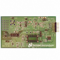
2.0 Board Assembly
The ADC121C02XEB evaluation board comes
fully assembled and ready for use. The provided
jumpers are in their recommended locations and
suit the needs of most users. Refer to the Bill of
Materials for a description of components, to
Figure 1 for major component placement, and to
Figure 10 for the evaluation board schematic.
While the board has been populated in a manner
that is most advantageous for typical usage, the
board can be customized by adding components
to meet the user’s specific needs.
comes ready to use with a DC coupled input
signal (Figure 2). However, by adding DC bias
resistors R1 and R4 (value 4.99kΩ), and changing
C1 to a 1.0uF capacitor, the board can be used
with an AC coupled input signal (Figure 3).
4
Figure 2: DC Coupled Input Configuration
Figure 3: AC Coupled Input Configuration
The board
If needed, the input can be terminated by adding
an appropriate termination resistor at R3. The
V_IN footprint (J2) has been stuffed with a single-
pin header for testing typical, slow-moving DC
input signals. An SMA footprint is also included
on the PCB and should be used for precise
dynamic performance evaluation.
Materials (Section 10) lists an appropriate SMA
connector to use.
The LMP7731 Low-noise, Precision Operational
Amplifier is included on the ADC121C02XEB for
convenient buffering of the analog input.
default, it is configured as a simple voltage
follower (Figure 4). Resistors R10 and R11 can
be modified to add non-inverting gain to the
circuit. Adding capacitance at C6 configures the
amplifier as a low-pass filter. To incorporate the
input buffer into the signal path, short pins 2 and 3
of JP1.
Figure 4: Input Buffer Configuration
http://www.national.com
The Bill of
By
Related parts for ADC121C02XEB/NOPB
Image
Part Number
Description
Manufacturer
Datasheet
Request
R

Part Number:
Description:
National Semiconductor [8-Bit D/A Converter]
Manufacturer:
National Semiconductor
Datasheet:
Part Number:
Description:
National Semiconductor [Media Coprocessor]
Manufacturer:
National Semiconductor
Datasheet:
Part Number:
Description:
Digitally Controlled Tone and Volume Circuit with Stereo Audio Power Amplifier, Microphone Preamp Stage and National 3D Sound
Manufacturer:
National Semiconductor
Datasheet:
Part Number:
Description:
Digitally Controlled Tone and Volume Circuit with Stereo Audio Power Amplifier, Microphone Preamp Stage and National 3D Sound
Manufacturer:
National Semiconductor
Datasheet:
Part Number:
Description:
AC97 Rev 2 Codec with Sample Rate Conversion and National 3D Sound
Manufacturer:
National Semiconductor
Part Number:
Description:
Manufacturer:
National Semiconductor
Datasheet:
Part Number:
Description:
Manufacturer:
National Semiconductor
Datasheet:
Part Number:
Description:
General Purpose, Low Voltage, Low Power, Rail-to-Rail Output Operational Amplifiers
Manufacturer:
National Semiconductor
Datasheet:
Part Number:
Description:
8-bit 20 MSPS flash A/D converter.
Manufacturer:
National Semiconductor
Datasheet:
Part Number:
Description:
Low Noise Quad Operational Amplifier
Manufacturer:
National Semiconductor
Datasheet:
Part Number:
Description:
Quad Differential Line Receivers
Manufacturer:
National Semiconductor
Datasheet:
Part Number:
Description:
Quad High Speed Trapezoidal? Bus Transceiver
Manufacturer:
National Semiconductor
Datasheet:
Part Number:
Description:
Dual Line Receiver
Manufacturer:
National Semiconductor
Datasheet:
Part Number:
Description:
TTL to 10k ECL Level Translator with Latch
Manufacturer:
National Semiconductor
Datasheet: