IRDC3637 International Rectifier, IRDC3637 Datasheet - Page 3
IRDC3637
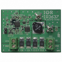
Manufacturer Part Number
IRDC3637
Description
BOARD EVAL SYNC BUCK REGULATOR
Manufacturer
International Rectifier
Datasheet
1.IR3637STRPBF.pdf
(21 pages)
Specifications of IRDC3637
Main Purpose
DC/DC, Step Down
Outputs And Type
1, Non-Isolated
Voltage - Output
1.8V
Current - Output
7A
Voltage - Input
4.5 ~ 5.5V
Regulator Topology
Buck
Frequency - Switching
400kHz
Board Type
Fully Populated
Utilized Ic / Part
IR3637
Lead Free Status / RoHS Status
Lead free / RoHS Compliant
Power - Output
-


PARAMETER
Error Amp
Fb Voltage Input Bias Current
Fb Voltage Input Bias Current
Transconductance
Oscillator
Frequency
Ramp-Amplitude Voltage
Output Drivers
Rise Time, Hdrv, Ldrv
Fall Time,Hdrv, Ldrv
Dead Band Time
Max Duty Cycle
Min Duty Cycle
PIN DESCRIPTIONS
PIN#
Rev. 1.1
06/16/05
1
2
3
4
5
6
7
8
PIN SYMBOL
SS / SD
Comp
HDrv
LDrv
Vcc
Gnd
Fb
Vc
This pin is connected directly to the output of the switching regulator via resistor divider to
set the output voltage and provide feedback to the error amplifier.
This pin provides biasing for the internal blocks of the IC as well as powers the low side
driver. A minimum of 0.1µF, high frequency capacitor must be connected from this pin to
ground to provide peak drive current capability.
Output driver for the synchronous power MOSFET.
IC's ground pin. This pin must be connected directly to the ground plane. A high frequency
capacitor (0.1 to 1µF) must be connected from Vcc and Vc pins to this pin for noise free
operation.
Output driver for the high side power MOSFET. The negative voltage at this pin may cause
instability for the gate drive circuit. To prevent this, a low forward voltage drop diode (e.g.
BAT54 or 1N4148) is required between this pin and ground.
This pin is connected to a voltage that must be at least 4V higher than the bus voltage
(assuming 5V threshold MOSFET) and powers the high side output driver. A minimum of
0.1µF, high frequency capacitor must be connected from this pin to ground to provide
peak drive current capability.
Compensation pin of the error amplifier. An external resistor and capacitor network is
typically connected from this pin to ground to provide loop compensation.
This pin provides user programmable soft-start function. Connect an extrnal capacitor
from this pin to ground to set the start up time of the output. The converter can be shut-
down by pulling this pin below 0.4V. During shutdown the upper FET is turned off and the
lower FET is turned on.
PIN DESCRIPTION
SYM
V
Freq
T
T
T
I
I
g
RAMP
FB1
FB2
T
OFF
T
ON
m
DB
r
f
SS=3V, Fb=0.6V
SS=0V, Fb=0.6V
C
C
Vcc=12V, 2V to 2V
Fb=0.6V, Freq=400kHz
Fb=1V
L
L
=1500pF, Vcc=12V,2V to 9V
=1500pF, Vcc=12V, 9V to 2V
TEST CONDITION
www.irf.com
MIN
450
360
40
81
TYP
1.25
-0.1
600
400
150
-64
30
30
85
IR3637SPBF
MAX
800
440
200
60
60
0
UNITS
µmho
kHz
µA
µA
ns
ns
ns
%
%
V
3
Related parts for IRDC3637
Image
Part Number
Description
Manufacturer
Datasheet
Request
R

Part Number:
Description:
SCHOTTKY RECTIFIER
Manufacturer:
International Rectifier Corp.
Datasheet:
Part Number:
Description:
SCHOTTKY RECTIFIER
Manufacturer:
International Rectifier Corp.
Datasheet:
Part Number:
Description:
SCHOTTKY RECTIFIER
Manufacturer:
International Rectifier Corp.
Datasheet:
Part Number:
Description:
SCHOTTKY RECTIFIER
Manufacturer:
International Rectifier Corp.
Datasheet:
Part Number:
Description:
SCHOTTKY RECTIFIER
Manufacturer:
International Rectifier Corp.
Datasheet:
Part Number:
Description:
SCHOTTKY RECTIFIER
Manufacturer:
International Rectifier Corp.
Datasheet:
Part Number:
Description:
SCHOTTKY RECTIFIER
Manufacturer:
International Rectifier Corp.
Datasheet:
Part Number:
Description:
SCHOTTKY RECTIFIER
Manufacturer:
International Rectifier Corp.
Datasheet:
Part Number:
Description:
SCHOTTKY RECTIFIER
Manufacturer:
International Rectifier Corp.
Datasheet:
Part Number:
Description:
SCHOTTKY RECTIFIER
Manufacturer:
International Rectifier Corp.
Datasheet:
Part Number:
Description:
SCHOTTKY RECTIFIER
Manufacturer:
International Rectifier Corp.
Datasheet:
Part Number:
Description:
SCHOTTKY RECTIFIER
Manufacturer:
International Rectifier Corp.
Datasheet:
Part Number:
Description:
SCHOTTKY RECTIFIER
Manufacturer:
International Rectifier Corp.
Datasheet:
Part Number:
Description:
SCHOTTKY RECTIFIER
Manufacturer:
International Rectifier Corp.
Datasheet:
Part Number:
Description:
SCHOTTKY RECTIFIER
Manufacturer:
International Rectifier Corp.
Datasheet: