NCP1203GEVB ON Semiconductor, NCP1203GEVB Datasheet - Page 5
NCP1203GEVB
Manufacturer Part Number
NCP1203GEVB
Description
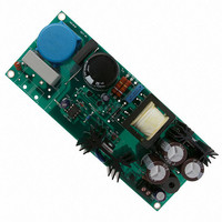
EVAL BOARD FOR NCP1203G
Manufacturer
ON Semiconductor
Specifications of NCP1203GEVB
Design Resources
NCP1203GEVB BOM NCP1203GEVB Gerber Files NCP1203 EVB Schematic
Main Purpose
AC/DC, Primary Side
Outputs And Type
1, Isolated
Voltage - Output
19V
Current - Output
4A
Voltage - Input
85 ~ 230VAC
Regulator Topology
Flyback
Frequency - Switching
60kHz
Board Type
Fully Populated
Utilized Ic / Part
NPC1200
Lead Free Status / RoHS Status
Lead free / RoHS Compliant
Power - Output
-
Lead Free Status / Rohs Status
Lead free / RoHS Compliant
For Use With/related Products
NCP1203G
Other names
NCP1203GEVBOS


to be in BCM at 180 VAC input voltage:
Lp +
a peak current of 2.36 A. The NCP1200 incorporates a
skip-cycle feature that forces the controller to slice the
switching pattern when the power supply drives light loads.
Depending on the system time constants, the recurrence of
the burst can enter the audible frequency range. Since the
default skip-cycle takes place at one third of maximum peak
current, it is better to avoid working at high peak current in
normal operation. Should noise still appear in skip mode,
pin1 lets you select a different lower skip level
(unfortunately to the detriment of the standby power)
generating less mechanical noise. As a result, we slightly
increased the primary inductance to 700 H to further limit
the noise in standby operation.
MOSFET Selection
maximum voltage of:
Figure 6. A Very Simple Way to Generate a
DRV
From the Flyback formula, we obtain:
Ip = primary peak current
N = Np / Ns = 1/0.166 = 6
Pout = output power
Lp = primary inductance
Fsw = switching frequency
Vf = secondary diode forward drop
VinDC Vac
Combining equations 14, 15 and 16 we obtain an Lp value
The numerical application gives a 484 H inductance with
The MOSFET drain voltage sees, in normal operation, a
CS
= efficiency
Ramp from a Square Wave Signal
( Vout 2 ) 2 @ Vout @ Vf ) Vf 2 ) @ ( eff @ N 2 @ Vin 2 )
VinDC max ) (Vout ) Vf) @ N ) Ip @
[ Pout @ [ (N @ Vout ) N @ Vf ) Vin) 2 @ F SW ]] @ 2
150
Radd1
Radd2
Ip +
2 (neglecting ripple)
R
2
1
C
h @ Lp @ F SW
2 @ Pout
D
R
sense
3
Clump
Lleak
http://onsemi.com
AND8076/D
500M
(16)
(17)
(18)
-2.00
1.50
4.50
3.50
2.50
14.0
10.0
6.00
2.00
Figure 7. Simulations Show a Capacitor Voltage Ramping
5
Up from a Few Hundred of mV Up to Nearly 5 V
10.0U
The first term represents the maximum rectified DC voltage
and goes up to 375 V. The reflected voltage pushes further
up by 101 V. Summing up these levels gives a total
steady-state drain voltage of 476 V. The last term in equation
18 depicts the leakage inductance action which further
stresses the MOSFET at the opening. If we select a 600 V
device, it leaves more than 100 V for this leakage action. A
clamping network will stop its rise anyway. A 2SK2843
from Toshiba can be a good choice. This is a TO-220 600 V
10 A component which features a 1.2
100 C.
Ramp Compensation
greater than 50%, we need to inject ramp compensation into
the controller to prevent subharmonic oscillations. An easy
way to generate a ramp, is to take the driving signal available
from pin5 and integrate it through a RC network. Figure 6
shows how to wire the components and Figure 7 shows the
signal obtain with a 18 k / 1 nF RC time constant.
methods exist. We will stick to the standard one which
consists in injecting between 50 and 75% of the off-time
downslope. The calculation is as follow:
R and Radd1 + Radd2. With a 11 V driving voltage delivered
by the NCP1200, we recommend a 18 k for R and 1 nF for
C. These values offer an acceptable tradeoff in terms of
power consumption but also in terms of noise immunity. The
With a supply entering CCM together with a duty-cycle
To calculate the necessary amount of ramp m, several
Primary off-slope:
Once reflected over Rsense, it becomes: 50.5 mV / s (S’)
Duty-cycle in CCM:
From Figure 6 network, the maximum voltage is given by
D +
N @ Vin ) Vout
30.0U
N @ (Vout ) Vf)
Vout
V
ramp
Lp
50.0U
+ 45% @ Vin + 120 VDC
+ 153 mA ms
70.0U
RDS
90.0U
(ON)
@ Tj =
(19)
(20)
Related parts for NCP1203GEVB
Image
Part Number
Description
Manufacturer
Datasheet
Request
R

Part Number:
Description:
Current Mode Controller Fixed Frequency Operation
Manufacturer:
ON Semiconductor
Datasheet:
Part Number:
Description:
ON Semiconductor [VOLTAGE REGULATOR]
Manufacturer:
ON Semiconductor
Datasheet:
Part Number:
Description:
357-036-542-201 CARDEDGE 36POS DL .156 BLK LOPRO
Manufacturer:
ON Semiconductor
Datasheet:
Part Number:
Description:
357-036-542-201 CARDEDGE 36POS DL .156 BLK LOPRO
Manufacturer:
ON Semiconductor
Datasheet:
Part Number:
Description:
357-036-542-201 CARDEDGE 36POS DL .156 BLK LOPRO
Manufacturer:
ON Semiconductor
Datasheet:
Part Number:
Description:
357-036-542-201 CARDEDGE 36POS DL .156 BLK LOPRO
Manufacturer:
ON Semiconductor
Datasheet:
Part Number:
Description:
357-036-542-201 CARDEDGE 36POS DL .156 BLK LOPRO
Manufacturer:
ON Semiconductor
Datasheet:
Part Number:
Description:
357-036-542-201 CARDEDGE 36POS DL .156 BLK LOPRO
Manufacturer:
ON Semiconductor
Datasheet:
Part Number:
Description:
357-036-542-201 CARDEDGE 36POS DL .156 BLK LOPRO
Manufacturer:
ON Semiconductor
Datasheet:
Part Number:
Description:
357-036-542-201 CARDEDGE 36POS DL .156 BLK LOPRO
Manufacturer:
ON Semiconductor
Datasheet:
Part Number:
Description:
357-036-542-201 CARDEDGE 36POS DL .156 BLK LOPRO
Manufacturer:
ON Semiconductor
Datasheet:
Part Number:
Description:
357-036-542-201 CARDEDGE 36POS DL .156 BLK LOPRO
Manufacturer:
ON Semiconductor
Datasheet:
Part Number:
Description:
Manufacturer:
ON Semiconductor
Datasheet:
Part Number:
Description:
Manufacturer:
ON Semiconductor
Datasheet: