MC34063LINVEVB ON Semiconductor, MC34063LINVEVB Datasheet
MC34063LINVEVB
Specifications of MC34063LINVEVB


Related parts for MC34063LINVEVB

MC34063LINVEVB Summary of contents
Page 1
MC34063A, MC33063A, SC34063A, SC33063A, NCV33063A 1.5 A, Step-Up/Down/ Inverting Switching Regulators The MC34063A Series is a monolithic control circuit containing the primary functions required for DC−to−DC converters. These devices consist of an internal temperature compensated reference, comparator, controlled duty cycle ...
Page 2
Switch 1 Collector Switch 2 Emitter Timing 3 Capacitor 4 GND (Top View) MAXIMUM RATINGS Rating Power Supply Voltage Comparator Input Voltage Range Switch Collector Voltage Switch Emitter Voltage ( Pin 1 Switch Collector to Emitter Voltage ...
Page 3
ELECTRICAL CHARACTERISTICS Characteristics OSCILLATOR Frequency ( 1.0 nF, T Pin Charge Current ( Discharge Current ( ...
Page 4
V = 5.0 V, Pin Pin 5 = GND 25° TIME (ms FREQUENCY (kHz 0.0 0.5 1.0 1.5 2.0 2.5 3.0 ...
Page 5
L 8 180 OSC 0. 100 + Comp 2.2 k Test Line Regulation Load ...
Page 6
Figure 10. External Current Boost Connections for I 9a. External NPN Switch 8. If the output switch is driven into hard saturation (non−Darlington configuration) at low switch currents (≤ 300 mA) and high ...
Page 7
0. 100 + - 1.2 k Test Line Regulation Load Regulation Output Ripple Short Circuit Current Efficiency Output Ripple With Optional Filter ...
Page 8
100 + - 5 R2 8.2 k Test Line Regulation Load Regulation Output Ripple Short Circuit Current Efficiency Output Ripple With Optional Filter 8 ...
Page 9
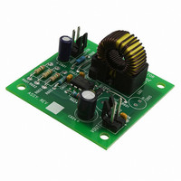
Figure 15. Printed Circuit Board and Component Layout (Circuits of Figures 9, 11, 13) INDUCTOR DATA Converter Inductance (mH) Step−Up 170 Step−Down 220 Voltage−Inverting 88 All inductors are wound on Magnetics Inc. 55117 toroidal core. http://onsemi.com 9 Turns/Wire 38 Turns ...
Page 10
Figure 16. Printed Circuit Board for DFN Device http://onsemi.com 10 ...
Page 11
Calculation Step− out ) off sat in(min off off off off t ...
Page 12
ORDERING INFORMATION Device MC33063AD MC33063ADG MC33063ADR2 MC33063ADR2G SC33063ADR2G MC33063AP1 MC33063AP1G MC33063AVD MC33063AVDG MC33063AVDR2 MC33063AVDR2G NCV33063AVDR2* NCV33063AVDR2G* MC33063AVP MC33063AVPG MC34063AD MC34063ADG MC34063ADR2 MC34063ADR2G SC34063ADR2G MC34063AP1 MC34063AP1G SC34063AP1G MC33063MNTXG †For information on tape and reel specifications, including part orientation and tape sizes, ...
Page 13
... G C SEATING PLANE −Z− 0.25 (0.010 *For additional information on our Pb−Free strategy and soldering details, please download the ON Semiconductor Soldering and Mounting Techniques Reference Manual, SOLDERRM/D. PACKAGE DIMENSIONS SOIC−8 NB CASE 751−07 ISSUE 0.10 (0.004 SOLDERING FOOTPRINT* 1 ...
Page 14
NOTE 5 F TOP VIEW e 0.010 SIDE VIEW PACKAGE DIMENSIONS PDIP− SUFFIX CASE 626−05 ISSUE M NOTES: 1. DIMENSIONING AND TOLERANCING PER ...
Page 15
... 0.05 C NOTE 3 *For additional information on our Pb−Free strategy and soldering details, please download the ON Semiconductor Soldering and Mounting Techniques Reference Manual, SOLDERRM/D. N. American Technical Support: 800−282−9855 Toll Free USA/Canada Europe, Middle East and Africa Technical Support: Phone: 421 33 790 2910 Japan Customer Focus Center Phone: 81− ...