NCP1422EVB ON Semiconductor, NCP1422EVB Datasheet - Page 3
NCP1422EVB
Manufacturer Part Number
NCP1422EVB
Description
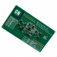
EVAL BOARD FOR NCP1422
Manufacturer
ON Semiconductor
Specifications of NCP1422EVB
Design Resources
NCP1422 EVB BOM NCP1422EVB Gerber Files NCP1422EVB Schematic
Main Purpose
DC/DC, Step Up
Outputs And Type
1, Non-Isolated
Voltage - Output
3.3 ~ 5 V
Current - Output
800mA
Voltage - Input
2.5V, 3.6V
Regulator Topology
Boost
Frequency - Switching
1.2MHz
Board Type
Fully Populated
Utilized Ic / Part
NCP1422
Lead Free Status / RoHS Status
Lead free / RoHS Compliant
Power - Output
-
Lead Free Status / Rohs Status
Lead free / RoHS Compliant
For Use With/related Products
NCP1422
Other names
NCP1422EVBOS


Maximum ratings are those values beyond which device damage can occur. Maximum ratings applied to the device are individual stress limit values
(not normal operating conditions) and are not valid simultaneously. If these limits are exceeded, device functional operation is not implied, damage
may occur and reliability may be affected.
1. This device contains ESD protection and exceeds the following tests:
2. The maximum package power dissipation limit must not be exceeded.
3. Latchup Current Maximum Rating: ±150 mA per JEDEC standard: JESD78.
4. Moisture Sensitivity Level: MSL 1 per IPC/JEDEC standard: J−STD−020A.
5. Measured on approximately 1x1 inch sq. of 1 oz. Copper.
PIN FUNCTION DESCRIPTIONS
MAXIMUM RATINGS
Power Supply (Pin 10)
Input/Output Pins (Pin 1−3, Pin 5−8)
Thermal Characteristics
Operating Junction Temperature Range
Operating Ambient Temperature Range
Storage Temperature Range
Pin
DFN−10 Plastic Package
Thermal Resistance Junction−to−Air (Note 5)
10
1
2
3
4
5
6
7
8
9
Human Body Model (HBM) ±2.0 kV per JEDEC standard: JESD22−A114. *Except OUT pin, which is 1k V.
Machine Model (MM) ±200 V per JEDEC standard: JESD22−A115. *Except OUT pin, which is 100 V.
Symbol
LBI/EN
GND
OUT
LBO
REF
BAT
NC
NC
FB
LX
P D +
(T
Output Voltage Feedback Input.
Low−Battery Detector Input and IC Enable. With this pin pulled down below 0.5 V, the device is disabled and
enters the shutdown mode.
Open−Drain Low−Battery Detector Output. Output is LOW when V
shutdown mode.
No Connect Pin
1.20 V Reference Voltage Output, bypass with 300 nF capacitor. If this pin is loaded, bypass with 1.0 mF
capacitor; this pin can be loaded up to 2.5 mA @ V
Battery input connection for internal ring−killer.
Ground.
N−Channel and P−Channel Power MOSFET drain connection.
No Connect Pin
Power Output. OUT also provides bootstrap power to the device.
A
T J(max) * T A
= 25°C unless otherwise noted.)
R qJA
Rating
http://onsemi.com
NCP1422
3
Description
OUT
= 3.3 V.
Symbol
V
R
T
V
LBI
P
OUT
T
T
stg
JA
IO
A
D
J
is < 1.20 V. LBO is high impedance in
−40 to +150
−55 to +150
−40 to +85
−0.3, 5.5
−0.3, 5.5
Value
1824
68.5
mW_
Unit
C/W
_C
_C
_C
V
V
Related parts for NCP1422EVB
Image
Part Number
Description
Manufacturer
Datasheet
Request
R

Part Number:
Description:
Sync-Rect PFM Step-Up DC-DC Converter
Manufacturer:
ON Semiconductor
Datasheet:
Part Number:
Description:
ON Semiconductor [VOLTAGE REGULATOR]
Manufacturer:
ON Semiconductor
Datasheet:
Part Number:
Description:
357-036-542-201 CARDEDGE 36POS DL .156 BLK LOPRO
Manufacturer:
ON Semiconductor
Datasheet:
Part Number:
Description:
357-036-542-201 CARDEDGE 36POS DL .156 BLK LOPRO
Manufacturer:
ON Semiconductor
Datasheet:
Part Number:
Description:
357-036-542-201 CARDEDGE 36POS DL .156 BLK LOPRO
Manufacturer:
ON Semiconductor
Datasheet:
Part Number:
Description:
357-036-542-201 CARDEDGE 36POS DL .156 BLK LOPRO
Manufacturer:
ON Semiconductor
Datasheet:
Part Number:
Description:
357-036-542-201 CARDEDGE 36POS DL .156 BLK LOPRO
Manufacturer:
ON Semiconductor
Datasheet:
Part Number:
Description:
357-036-542-201 CARDEDGE 36POS DL .156 BLK LOPRO
Manufacturer:
ON Semiconductor
Datasheet:
Part Number:
Description:
357-036-542-201 CARDEDGE 36POS DL .156 BLK LOPRO
Manufacturer:
ON Semiconductor
Datasheet:
Part Number:
Description:
357-036-542-201 CARDEDGE 36POS DL .156 BLK LOPRO
Manufacturer:
ON Semiconductor
Datasheet:
Part Number:
Description:
357-036-542-201 CARDEDGE 36POS DL .156 BLK LOPRO
Manufacturer:
ON Semiconductor
Datasheet:
Part Number:
Description:
357-036-542-201 CARDEDGE 36POS DL .156 BLK LOPRO
Manufacturer:
ON Semiconductor
Datasheet:
Part Number:
Description:
Manufacturer:
ON Semiconductor
Datasheet:
Part Number:
Description:
Manufacturer:
ON Semiconductor
Datasheet: