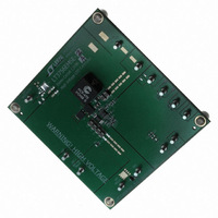
DC1319B-A Linear Technology, DC1319B-A Datasheet - Page 14

DC1319B-A
Manufacturer Part Number
DC1319B-A
Description
BOARD EVAL LED DRIVER LT3756
Manufacturer
Linear Technology
Specifications of DC1319B-A
Current - Output / Channel
500mA
Outputs And Type
1, Non-Isolated
Voltage - Output
100V
Features
Dimmable
Voltage - Input
8 ~ 80V
Utilized Ic / Part
LT3756
Lead Free Status / RoHS Status
Lead free / RoHS Compliant
Other names
DC1319A-A
DC1319A-A
DC1319A-A
applicaTions inForMaTion
LT3756/LT3756-1/LT3756-2
important when operating at high ambient temperatures.
The majority of the power dissipation in the IC comes from
the supply current needed to drive the gate capacitance of
the external power MOSFET. This gate drive current can
be calculated as:
A low Q
erating at high input voltages, and the switching frequency
should also be chosen carefully to ensure that the IC does
not exceed a safe junction temperature. The internal junc-
tion temperature of the IC can be estimated by:
where T
current of the part (maximum 1.5mA) and θ
package thermal impedance (68°C/W for the 3mm × 3mm
QFN package). For example, an application with T
= 85°C, V
with Q
will be approximately:
The exposed pad on the bottom of the package must be
soldered to a ground plane. This ground should then be
connected to an internal copper ground plane with thermal
vias placed directly under the package to spread out the
heat dissipated by the IC.
If LT3756 junction temperature reaches 165°C, the GATE
and PWMOUT pins will be driven to GND and the soft-
start (SS) pin will be discharged to GND. Switching will
be enabled after device temperature is reduced 10°C. This
function is intended to protect the device during momentary
thermal overload conditions.
Frequency Synchronization (LT3756-1 Only)
The LT3756-1 switching frequency can be synchronized to
an external clock using the SYNC pin. For proper operation,
the R
20% lower than the external clock frequency. The SYNC
pin is disabled during the soft-start period.
Observation of the following guidelines about the SYNC
waveform will ensure proper operation of this feature.
I
T
T
GATE
J
J
T
= 85°C + [60V (1.5mA + 400kHz • 20nC) • 68°C/W]
= 124°C
= T
resistor should be chosen for a switching frequency
G
G
A
= f
A
= 20nC, the maximum IC junction temperature
power MOSFET should always be used when op-
is the ambient temperature, I
IN(MAX)
+ [V
SW
• Q
IN
(I
= 60V, f
G
Q
+ f
SW
SW
• Q
= 400kHz, and having a FET
G
) • θ
JA
]
Q
is the quiescent
JA
A(MAX)
is the
Driving SYNC with a 50% duty cycle waveform is always
a good choice, otherwise, maintain the duty cycle between
20% and 60%. When using both PWM and SYNC features,
the PWM signal rising edge should occur at least 200ns
before the SYNC rising edge (V
performance. If the SYNC pin is not used, it should be
connected to GND.
Open LED Detection (LT3756 and LT3756-2)
The LT3756 and LT3756-2 provide an open-collector status
pin, OPENLED, that pulls low when the FB pin is within
~50mV of its 1.25V regulated voltage. If the open LED
clamp voltage is programmed correctly using the FB pin,
then the FB pin should never exceed 1.1V when LEDs are
connected, therefore, the only way for the FB pin to be
within 50mV of the regulation voltage is for an open LED
event to have occurred. The key difference between the
LT3756 and LT3756-2 is the behavior of the OPENLED pin
when the FB pin crosses and re-crosses the FB overvoltage
threshold at 1.31V (typ). The LT3756-2 asserts/de-asserts
OPENLED freely when crossing the 1.31V threshold.
The LT3756, by comparison, de-asserts OPENLED when
FB exceeds 1.31V and is prevented from re-asserting
OPENLED until the FB pin falls below the 1.2V (typ) open
LED threshold and clears the fault. The LT3756-2 has the
more general purpose behavior and is recommended for
applications using OPENLED.
Input Capacitor Selection
The input capacitor supplies the transient input current for
the power inductor of the converter and must be placed
and sized according to the transient current requirements.
The switching frequency, output current and tolerable input
voltage ripple are key inputs to estimating the capacitor
value. An X7R type ceramic capacitor is usually the best
choice since it has the least variation with temperature
and DC bias. Typically, boost and SEPIC converters re-
quire a lower value capacitor than a buck mode converter.
Assuming that a 100mV input voltage ripple is acceptable,
the required capacitor value for a boost converter can be
estimated as follows:
C
IN
(µF) =I
LED
(A) •
V
V
OUT
IN
• t
SW
(µs) •
IH
) for optimal PWM
A • µs
1µF
375612fb


