DC1319B-A Linear Technology, DC1319B-A Datasheet - Page 7
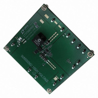
DC1319B-A
Manufacturer Part Number
DC1319B-A
Description
BOARD EVAL LED DRIVER LT3756
Manufacturer
Linear Technology
Specifications of DC1319B-A
Current - Output / Channel
500mA
Outputs And Type
1, Non-Isolated
Voltage - Output
100V
Features
Dimmable
Voltage - Input
8 ~ 80V
Utilized Ic / Part
LT3756
Lead Free Status / RoHS Status
Lead free / RoHS Compliant
Other names
DC1319A-A
DC1319A-A
DC1319A-A


Typical perForMance characTerisTics
PWMOUT (Pin 1/Pin 11): Buffered Version of PWM Signal
for Driving LED Load Disconnect NMOS or Level Shift.
This pin also serves in a protection function for the FB
overvoltage condition—will toggle if the FB input is greater
than the FB regulation voltage (V
The PWMOUT pin is driven from INTV
gate cut-off voltage higher than 1V is recommended.
FB (Pin 2/Pin 12): Voltage Loop Feedback Pin. FB is
intended for constant-voltage regulation or for LED protec-
tion/open LED detection. The internal transconductance
amplifier with output VC will regulate FB to 1.25V (nominal)
through the DC/DC converter. If the FB input is regulating
the loop, the OPENLED pull-down is asserted. This ac-
tion may signal an open LED fault. If FB is driven above
the FB threshold (by an external power supply spike, for
example), the OPENLED pull-down will be de-asserted and
the PWMOUT pin will be driven low to protect the LEDs
from an overcurrent event. Do not leave the FB pin open.
If not used, connect to GND.
pin FuncTions
40
30
20
10
0
0
ISP/ISN Input Bias Current
vs CTRL Voltage
0.5
(MSOP/QFN)
CTRL (V)
1
FB
) plus 60mV (typical).
ISP
ISN
CC
. Use of a FET with
1.5
375612 G19
2
ISN (Pin 3/Pin 13): Connection Point for the Negative
Terminal of the Current Feedback Resistor. If ISN is greater
than 2.9V, the LED current can be programmed by I
100mV/R
(10 • R
cally 25µA. Below 3V, ISN is an input to the short-circuit
protection feature that forces GATE to 0V if ISP exceeds
ISN by more than 150mV (typ).
ISP (Pin 4/Pin 14): Connection Point for the Positive
Terminal of the Current Feedback Resistor. Input bias
current is dependent upon CTRL pin voltage as shown
in the TPC. ISP is an input to the short-circuit protection
feature when ISN is less than 3V.
VC (Pin 5/Pin 15): Transconductance Error Amplifier
Output Pin Used to Stabilize the Voltage Loop with an RC
Network. This pin is high impedance when PWM is low, a
feature that stores the demand current state variable for
the next PWM high transition. Connect a capacitor between
this pin and GND; a resistor in series with the capacitor is
recommended for fast transient response.
LT3756/LT3756-1/LT3756-2
–0.5
–2.5
–1.0
–1.5
–2.0
0
LED
0
INTV
vs Current, Temperature
V
LED
IN
) when V
T
= 7V
A
CC
when V
= 25°C, unless otherwise noted.
3
Dropout Voltage
LDO CURRENT (mA)
CTRL
CTRL
6
150°C
> 1.2V or I
≤ 1V. Input bias current is typi-
9
–45°C
25°C
125°C
12
375612 G20
LED
15
= (V
CTRL
–100mV)/
375612fb
LED
=
Related parts for DC1319B-A
Image
Part Number
Description
Manufacturer
Datasheet
Request
R

Part Number:
Description:
CD ROM LINEARVIEW DATASHEETS
Manufacturer:
Linear Technology

Part Number:
Description:
Standalone Linear Li-Ion Battery Charger with Thermal Regulation in ThinSOT
Manufacturer:
Linear Technology Corporation
Datasheet:
Part Number:
Description:
Low noise, high frequency, 8th order linear phase lowpass filter
Manufacturer:
Linear Technology Corporation
Datasheet:
Part Number:
Description:
Manufacturer:
Linear Technology Corporation
Datasheet:
Part Number:
Description:
Manufacturer:
Linear Technology Corporation
Datasheet:
Part Number:
Description:
Manufacturer:
Linear Technology Corporation
Datasheet:
Part Number:
Description:
Manufacturer:
Linear Technology Corporation
Datasheet:
Part Number:
Description:
Manufacturer:
Linear Technology Corporation
Datasheet:
Part Number:
Description:
Manufacturer:
Linear Technology Corporation
Datasheet:
Part Number:
Description:
Manufacturer:
Linear Technology Corporation
Datasheet:
Part Number:
Description:
Dual and Quad, JFET Input Precision High Speed Op Amps
Manufacturer:
Linear Technology Corporation
Datasheet:
Part Number:
Description:
Manufacturer:
Linear Technology Corporation
Datasheet:
Part Number:
Description:
1, 2, 6 and 8 Channel, 10-Bit Serial I/O Data Acquisition Systems
Manufacturer:
Linear Technology Corporation
Datasheet:
Part Number:
Description:
Manufacturer:
Linear Technology Corporation
Datasheet:
Part Number:
Description:
Universal dual filter building block
Manufacturer:
Linear Technology Corporation
Datasheet: