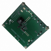
DC1319B-A Linear Technology, DC1319B-A Datasheet - Page 8
DC1319B-A
Manufacturer Part Number
DC1319B-A
Description
BOARD EVAL LED DRIVER LT3756
Manufacturer
Linear Technology
Specifications of DC1319B-A
Current - Output / Channel
500mA
Outputs And Type
1, Non-Isolated
Voltage - Output
100V
Features
Dimmable
Voltage - Input
8 ~ 80V
Utilized Ic / Part
LT3756
Lead Free Status / RoHS Status
Lead free / RoHS Compliant
Other names
DC1319A-A
DC1319A-A
DC1319A-A


LT3756/LT3756-1/LT3756-2
pin FuncTions
CTRL (Pin 6/Pin 16): Current Sense Threshold Adjustment
Pin. Regulating threshold V
an offset for 0V < V
sense threshold is constant at the full-scale value of 100mV.
For 1V < V
threshold upon V
to a constant value, reaching 98% of full-scale value by
V
V
2V. This pin drives a resistor divider for the CTRL pin, either
for analog dimming or for temperature limit/compensation
of LED load. Can supply up to 100μA.
PWM (Pin 8/Pin 2): A signal low turns off switcher, idles
oscillator and disconnects VC pin from all internal loads.
PWMOUT pin follows PWM pin. PWM has an internal
pull-down resistor. If not used, connect to INTV
OPENLED (Pin 9/Pin 3, LT3756 and LT3756-2): An open-
collector pull-down on OPENLED asserts if the FB input
is greater than the FB regulation threshold minus 50mV
(typical). To function, the pin requires an external pull-up
current less than 1mA. When the PWM input is low and
the DC/DC converter is idle, the OPENLED condition is
latched to the last valid state when the PWM input was
high. When PWM input goes high again, the OPENLED
pin will be updated. This pin may be used to report an
open LED fault.
SYNC (Pin 9/Pin 3, LT3756-1 Only): The SYNC pin is used
to synchronize the internal oscillator to an external logic
level signal. The R
an internal switching frequency 20% slower than the SYNC
pulse frequency. Gate turn-on occurs a fixed delay after
the rising edge of SYNC. For best PWM performance, the
PWM rising edge should occur at least 200ns before the
SYNC rising edge. Use a 50% duty cycle waveform to drive
this pin. This pin replaces OPENLED on LT3756-1 option
parts. If not used, tie this pin to GND.
SS (Pin 10/Pin 4): Soft-Start Pin. This pin modulates
oscillator frequency and compensation pin voltage (VC)
clamp. The soft-start interval is set with an external capaci-
tor. The pin has a 10µA (typical) pull-up current source
to an internal 2.5V rail. The soft-start pin is reset to GND
REF
CTRL
(Pin 7/Pin 1): Voltage Reference Output Pin, Typically
= 1.1V. Do not leave this pin open.
CTRL
< 1.2V, the dependence of current sense
CTRL
T
CTRL
resistor should be chosen to program
transitions from a linear function
< 1V. For V
(ISP – ISN)
CTRL
is 1/10th V
> 1.2V the current
CTRL
CC
.
plus
by an undervoltage condition (detected by SHDN/UVLO
pin) or thermal limit.
RT (Pin 11/Pin 5): Switching Frequency Adjustment Pin.
Set the frequency using a resistor to GND (for resistor
values, see the Typical Performance curve or Table 1).
Do not leave the RT pin open.
SHDN/UVLO (Pin 12/Pin 6): Shutdown and Undervoltage
Detect Pin. An accurate 1.22V falling threshold with ex-
ternally programmable hysteresis detects when power is
OK to enable switching. Rising hysteresis is generated
by the external resistor divider and an accurate internal
2.1µA pull-down current. Above the threshold (but below
6V), SHDN/UVLO input bias current is sub-µA. Below the
falling threshold, a 2.1µA pull-down current is enabled so
the user can define the hysteresis with the external resis-
tor selection. An undervoltage condition resets soft-start.
Tie to 0.4V, or less, to disable the device and reduce V
quiescent current below 1µA.
INTV
Loads, GATE Driver and PWMOUT Driver. Supplied from
V
bypassed with a 4.7µF capacitor placed close to the pin.
Connect INTV
or equal to 8V.
V
bypassed with a 0.22µF (or larger) capacitor placed close
to the IC.
SENSE (Pin 15/Pin 9): The current sense input for the
control loop. Kelvin connect this pin to the positive ter-
minal of the switch current sense resistor, R
source of the NFET. The negative terminal of the current
sense resistor should be connected to the GND plane
close to the IC.
GATE (Pin 16/Pin 10): N-channel FET Gate Driver Output.
Switches between INTV
shutdown, fault or idle states.
GND (Pin 17/Pin 17): Ground. This pin also serves as
current sense input for control loop, sensing negative
terminal of current sense resistor. Solder the exposed pad
directly to ground plane.
IN
IN
and regulates to 7.15V (typical). INTV
(Pin 14/Pin 8): Input Supply Pin. Must be locally
CC
(Pin 13/Pin 7): Regulated Supply for Internal
CC
directly to V
CC
and GND. Driven to GND during
IN
if V
IN
is always less than
SENSE
CC
must be
, in the
375612fb
IN
Related parts for DC1319B-A
Image
Part Number
Description
Manufacturer
Datasheet
Request
R

Part Number:
Description:
CD ROM LINEARVIEW DATASHEETS
Manufacturer:
Linear Technology

Part Number:
Description:
Standalone Linear Li-Ion Battery Charger with Thermal Regulation in ThinSOT
Manufacturer:
Linear Technology Corporation
Datasheet:
Part Number:
Description:
Low noise, high frequency, 8th order linear phase lowpass filter
Manufacturer:
Linear Technology Corporation
Datasheet:
Part Number:
Description:
Manufacturer:
Linear Technology Corporation
Datasheet:
Part Number:
Description:
Manufacturer:
Linear Technology Corporation
Datasheet:
Part Number:
Description:
Manufacturer:
Linear Technology Corporation
Datasheet:
Part Number:
Description:
Manufacturer:
Linear Technology Corporation
Datasheet:
Part Number:
Description:
Manufacturer:
Linear Technology Corporation
Datasheet:
Part Number:
Description:
Manufacturer:
Linear Technology Corporation
Datasheet:
Part Number:
Description:
Manufacturer:
Linear Technology Corporation
Datasheet:
Part Number:
Description:
Dual and Quad, JFET Input Precision High Speed Op Amps
Manufacturer:
Linear Technology Corporation
Datasheet:
Part Number:
Description:
Manufacturer:
Linear Technology Corporation
Datasheet:
Part Number:
Description:
1, 2, 6 and 8 Channel, 10-Bit Serial I/O Data Acquisition Systems
Manufacturer:
Linear Technology Corporation
Datasheet:
Part Number:
Description:
Manufacturer:
Linear Technology Corporation
Datasheet:
Part Number:
Description:
Universal dual filter building block
Manufacturer:
Linear Technology Corporation
Datasheet: