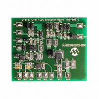
TC1016/17EV Microchip Technology, TC1016/17EV Datasheet - Page 2

TC1016/17EV
Manufacturer Part Number
TC1016/17EV
Description
BOARD DEMO FOR TC1016/TC1017
Manufacturer
Microchip Technology
Specifications of TC1016/17EV
Design Resources
TC1016/17EV Gerber Files
Channels Per Ic
1 - Single
Voltage - Output
1.8V, 3V
Current - Output
150mA, 150mA
Voltage - Input
2.7 ~ 6V
Regulator Type
Positive Fixed
Operating Temperature
-40°C ~ 125°C
Board Type
Fully Populated
Utilized Ic / Part
TC1016, TC1017
Processor To Be Evaluated
TC1016 and TC1017
Lead Free Status / RoHS Status
Contains lead / RoHS non-compliant
Lead Free Status / RoHS Status
Lead free / RoHS Compliant, Contains lead / RoHS non-compliant
TC1017
1.0
Absolute Maximum Ratings †
Input Voltage ....................................................................6.5V
Power Dissipation ......................... Internally Limited (Note 7)
Maximum Voltage On Any Pin ..................V
† Notice: Stresses above those listed under "Maximum
Ratings" may cause permanent damage to the device. This is
a stress rating only and functional operation of the device at
those or any other conditions above those indicated in the
operation listings of this specification is not implied. Exposure
to maximum rating conditions for extended periods may affect
device reliability.
ELECTRICAL CHARACTERISTICS
DS21813D-page 2
Electrical Specifications: Unless otherwise noted, V
Boldface type specifications apply for junction temperatures of –40°C to +125°C.
Input Operating Voltage
Maximum Output Current
Output Voltage
V
Line Regulation
Load Regulation (Note 4)
Dropout Voltage (Note 5)
Supply Current
Shutdown Supply Current
Power Supply Rejection Ratio
Wake-Up Time
(from Shutdown Mode)
Note 1:
OUT
Temperature Coefficient
2:
3:
4:
5:
6:
7:
8:
ELECTRICAL
CHARACTERISTICS
Parameter
The minimum V
V
Regulation is measured at a constant junction temperature using low duty-cycle pulse testing. Load regulation is tested
over a load range from 0.1 mA to the maximum specified output current. Changes in output voltage due to heating
effects are covered by the thermal regulation specification.
Dropout voltage is defined as the input-to-output differential at which the output voltage drops 2% below its nominal
value at a 1V differential.
Thermal regulation is defined as the change in output voltage at a time T after a change in power dissipation is applied,
excluding load or line regulation effects. Specifications are for a current pulse equal to I
The maximum allowable power dissipation is a function of ambient temperature, the maximum allowable junction
temperature and the thermal resistance from junction-to-air (i.e., T
dissipation causes the device to initiate thermal shutdown. Please see Section 5.1 “Thermal Shutdown”, for more
details
Output current is limited to 120 mA (typ) when V
TCV
R
is the regulator voltage setting. For example: V
OUT
.
=
------------------------------------------------------------------------------------- -
V OUTMAX V OUTMIN
IN
has to meet two conditions: V
V
OUT
V
–
V
OUT
V
I
TCV
IN
OUTMAX
PSRR
OUT
V
I
Sym
INSD
V
– V
t
/ V
OUT
I
WK
IN
IN
OUT
T
IN
| / V
OUT
IN
+ 0.3V to -0.3V
)| / V
R
10
R
6
IN
V
R
= V
Min
150
– 2.5%
2.7
—
—
—
—
—
—
—
—
—
—
—
R
IN
OUT
+ 1V, I
R
2.7V and V
= 1.8V, 2.7V, 2.8V, 3.0V.
is less than 0.5V due to a load fault or short-circuit condition.
L
V
= 100 µA, C
R
PIN FUNCTION TABLE
SHDN
NC
GND
V
V
0.04
0.38
0.05
Typ
180
285
Name
±0.5%
40
90
53
58
10
—
—
OUT
IN
2
IN
A
(V
, T
R
Shutdown control input.
No connect
Ground terminal
Regulated voltage output
Unregulated supply input
L
J
,
+ 2.5%) + V
V
= 1.0 µF, SHDN > V
R
JA
Max
+ 2.5%
200
350
500
). Exceeding the maximum allowable power
6.0
0.2
1.5
90
—
—
—
—
—
2
DROPOUT
ppm/°C Note 3
© 2005 Microchip Technology Inc.
Units
LMAX
%/V
mA
mV
µA
µA
dB
µs
%
V
V
Function
.
IH
at V
, T
Note 1
Note 2
(V
I
I
I
I
I
SHDN = V
SHDN = 0V
f =1 kHz, I
V
C
f = 100 Hz
L
L
L
L
L
A
IN
IN
IN
R
= 0.1 mA to I
= 100 µA
= 50 mA
= 100 mA
= 150 mA
= +25°C
= 6V for t = 10 msec.
Test Conditions
= 5V, I
+ 1V) < V
= C
OUT
L
L
IH
= 50 mA
= 60 mA,
=1 µF,
, I
IN
L
OUTMAX
= 0
< 6V


