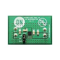
NCP690MN50T2GEVB ON Semiconductor, NCP690MN50T2GEVB Datasheet

NCP690MN50T2GEVB
Specifications of NCP690MN50T2GEVB
Related parts for NCP690MN50T2GEVB
NCP690MN50T2GEVB Summary of contents
Page 1
NCP690, NCP691, NCP692 1 A, Low I , Very Low GND Dropout Regulator (VLDO) with/without Enable The NCP690, NCP691, NCP692 CMOS LDO family provides output current with enhanced ESD in either fixed voltage options or an adjustable ...
Page 2
V IN 1,6 IN NCP692 3 EN* GND mF** Note: * NCP692 device has EN active high Note: ** Minimum value required for stability Figure 1. NCP692 Typical Application Circuit for Fixed Version (Output voltage versions: 1.5 ...
Page 3
IN MOSFET DRIVER WITH CURRENT LIMIT THERMAL N/C SHUTDOWN GND Figure 5. NCP690 Block Diagram (Fixed Version) IN MOSFET DRIVER WITH CURRENT LIMIT THERMAL SHUTDOWN EN GND Figure 6. NCP691 Block Diagram (Fixed Version) IN MOSFET DRIVER WITH CURRENT LIMIT ...
Page 4
IN MOSFET DRIVER WITH CURRENT LIMIT THERMAL N/C SHUTDOWN GND Figure 8. NCP690 Block Diagram (Adjustable Version) IN MOSFET DRIVER WITH CURRENT LIMIT THERMAL EN SHUTDOWN GND Figure 9. NCP691 Block Diagram (Adjustable Version) IN MOSFET DRIVER WITH CURRENT LIMIT ...
Page 5
Table 3. ABSOLUTE MAXIMUM RATINGS Rating Input Voltage (Note 1) Chip Enable Voltage Output Voltage Output Voltage / Sense Input, (SNS pin) Electrostatic Discharge Maximum Junction Temperature Storage Temperature Range Stresses exceeding Maximum Ratings may damage the device. Maximum Ratings ...
Page 6
Table 6. ELECTRICAL CHARACTERISTICS values T = 25°C, for Min/Max values T = −40°C to 125°C; unless otherwise noted. (Note Parameter Output voltage V IN (Adjustable Version) I OUT Output voltage (Fixed Version ...
Page 7
Table 6. ELECTRICAL CHARACTERISTICS values T = 25°C, for Min/Max values T = −40°C to 125°C; unless otherwise noted. (Note 5) (continued Parameter Power supply ripple rejection V OUT (Note Output ...
Page 8
OUT_NOM 5.03 IN OUT 5.02 5. 100 mA OUT 5.00 4.99 4. OUT 4.97 4.96 −40 − ...
Page 9
RMS IN 3.0 V OUT C IN 2.5 I OUT T A 2.0 1.5 1.0 0 100 1000 FREQUENCY (Hz) Figure 21. Noise Density vs. Frequency (V = 5.0 V) out ...
Page 10
mF, IN OUT 4. rise TIME (50 ms/DIV) Figure 27. Line Transient (V = 5.0 V) out V EN 3.5 3.0 2.5 V OUT 2.0 1.5 V 1.0 IN ...
Page 11
Load Regulation The change in output voltage for a change in output load current at a constant temperature. Dropout Voltage The input/output differential at which the regulator output no longer maintains regulation against further reductions in input voltage. Measured, when ...
Page 12
Figure 4. The output voltage and resistors should be chosen using Equations 1 and 1.250 OUT ADJ ...
Page 13
DEVICE ORDERING INFORMATION Nominal Output Voltage Device NCP690MN15T2G NCP690MN18T2G NCP690MN25T2G NCP690MN33T2G NCP690MN50T2G NCP690MNADJT2G NCP691MN15T2G NCP691MN18T2G NCP691MN25T2G NCP691MN33T2G NCP691MN50T2G NCP691MNADJT2G NCP692MN15T2G NCP692MN18T2G NCP692MN25T2G NCP692MN33T2G NCP692MN50T2G NCP692MNADJT2G †For information on tape and reel specifications, including part orientation and tape sizes, please refer ...
Page 14
... C 0.63 0.025 *For additional information on our Pb−Free strategy and soldering details, please download the ON Semiconductor Soldering and Mounting Techniques Reference Manual, SOLDERRM/D. N. American Technical Support: 800−282−9855 Toll Free USA/Canada Europe, Middle East and Africa Technical Support: Phone: 421 33 790 2910 Japan Customer Focus Center Phone: 81− ...


