C8051F120DK Silicon Laboratories Inc, C8051F120DK Datasheet - Page 10
C8051F120DK
Manufacturer Part Number
C8051F120DK
Description
DEVKIT-F120/21/22/23/24/25/26/27
Manufacturer
Silicon Laboratories Inc
Type
MCUr
Datasheet
1.C8051F120DK.pdf
(350 pages)
Specifications of C8051F120DK
Contents
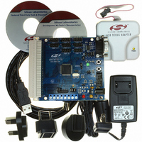
Evaluation Board, Power Supply, USB Cables, Adapter and Documentation
Processor To Be Evaluated
C8051F12x and C8051F13x
Interface Type
USB
Silicon Manufacturer
Silicon Labs
Core Architecture
8051
Silicon Core Number
C8051F120
Silicon Family Name
C8051F12x
Lead Free Status / RoHS Status
Contains lead / RoHS non-compliant
For Use With/related Products
C8051F120, 121, 122, 123, 124, 125, 126, 127
Lead Free Status / Rohs Status
Lead free / RoHS Compliant
Other names
336-1224
Available stocks
Company
Part Number
Manufacturer
Quantity
Price
Company:

Part Number:
C8051F120DK
Manufacturer:
SiliconL
Quantity:
4


C8051F120/1/2/3/4/5/6/7
C8051F130/1/2/3
6. ADC0 (10-Bit ADC, C8051F122/3/6/7 and C8051F13x Only)
7. ADC2 (8-Bit ADC, C8051F12x Only)
8. DACs, 12-Bit Voltage Mode (C8051F12x Only)
9. Voltage Reference
10. Comparators
11. CIP-51 Microcontroller
12. Multiply And Accumulate (MAC0)
10
Figure 6.1. 10-Bit ADC0 Functional Block Diagram ................................................. 73
Figure 6.2. Typical Temperature Sensor Transfer Function..................................... 74
Figure 6.3. ADC0 Track and Conversion Example Timing....................................... 76
Figure 6.4. ADC0 Equivalent Input Circuits.............................................................. 77
Figure 6.5. ADC0 Data Word Example .................................................................... 83
Figure 6.6. 10-Bit ADC0 Window Interrupt Example:
Figure 6.7. 10-Bit ADC0 Window Interrupt Example:
Figure 6.8. 10-Bit ADC0 Window Interrupt Example:
Figure 6.9. 10-Bit ADC0 Window Interrupt Example:
Figure 7.1. ADC2 Functional Block Diagram............................................................ 91
Figure 7.2. ADC2 Track and Conversion Example Timing....................................... 93
Figure 7.3. ADC2 Equivalent Input Circuit................................................................ 94
Figure 7.4. ADC2 Data Word Example .................................................................... 99
Figure 7.5. ADC2 Window Compare Examples, Single-Ended Mode.................... 100
Figure 7.6. ADC2 Window Compare Examples, Differential Mode ........................ 101
Figure 8.1. DAC Functional Block Diagram............................................................ 105
Figure 9.1. Voltage Reference Functional Block Diagram (C8051F120/2/4/6) ...... 114
Figure 9.2. Voltage Reference Functional Block Diagram (C8051F121/3/5/7) ...... 115
Figure 9.3. Voltage Reference Functional Block Diagram (C8051F130/1/2/3) ...... 117
Figure 10.1. Comparator Functional Block Diagram .............................................. 119
Figure 10.2. Comparator Hysteresis Plot ............................................................... 121
Figure 11.1. CIP-51 Block Diagram....................................................................... 128
Figure 11.2. Memory Map ...................................................................................... 133
Figure 11.3. Address Memory Map for Instruction Fetches (128 kB Flash Only)... 134
Figure 11.4. SFR Page Stack................................................................................. 137
Figure 11.5. SFR Page Stack While Using SFR Page 0x0F To Access Port 5...... 138
Figure 11.6. SFR Page Stack After ADC2 Window Comparator Interrupt Occurs . 139
Figure 11.7. SFR Page Stack Upon PCA Interrupt Occurring During an ADC2 ISR 140
Figure 11.8. SFR Page Stack Upon Return From PCA Interrupt ........................... 140
Figure 11.9. SFR Page Stack Upon Return From ADC2 Window Interrupt ........... 141
Figure 12.1. MAC0 Block Diagram ......................................................................... 165
Figure 12.2. Integer Mode Data Representation .................................................... 166
Figure 12.3. Fractional Mode Data Representation................................................ 166
Figure 12.4. MAC0 Pipeline.................................................................................... 167
Right Justified Single-Ended Data ......................................................... 86
Right Justified Differential Data ............................................................. 87
Left Justified Single-Ended Data ........................................................... 88
Left Justified Differential Data................................................................ 89
Rev. 1.4
Related parts for C8051F120DK
Image
Part Number
Description
Manufacturer
Datasheet
Request
R

Part Number:
Description:
SMD/C°/SINGLE-ENDED OUTPUT SILICON OSCILLATOR
Manufacturer:
Silicon Laboratories Inc
Part Number:
Description:
Manufacturer:
Silicon Laboratories Inc
Datasheet:
Part Number:
Description:
N/A N/A/SI4010 AES KEYFOB DEMO WITH LCD RX
Manufacturer:
Silicon Laboratories Inc
Datasheet:
Part Number:
Description:
N/A N/A/SI4010 SIMPLIFIED KEY FOB DEMO WITH LED RX
Manufacturer:
Silicon Laboratories Inc
Datasheet:
Part Number:
Description:
N/A/-40 TO 85 OC/EZLINK MODULE; F930/4432 HIGH BAND (REV E/B1)
Manufacturer:
Silicon Laboratories Inc
Part Number:
Description:
EZLink Module; F930/4432 Low Band (rev e/B1)
Manufacturer:
Silicon Laboratories Inc
Part Number:
Description:
I°/4460 10 DBM RADIO TEST CARD 434 MHZ
Manufacturer:
Silicon Laboratories Inc
Part Number:
Description:
I°/4461 14 DBM RADIO TEST CARD 868 MHZ
Manufacturer:
Silicon Laboratories Inc
Part Number:
Description:
I°/4463 20 DBM RFSWITCH RADIO TEST CARD 460 MHZ
Manufacturer:
Silicon Laboratories Inc
Part Number:
Description:
I°/4463 20 DBM RADIO TEST CARD 868 MHZ
Manufacturer:
Silicon Laboratories Inc
Part Number:
Description:
I°/4463 27 DBM RADIO TEST CARD 868 MHZ
Manufacturer:
Silicon Laboratories Inc
Part Number:
Description:
I°/4463 SKYWORKS 30 DBM RADIO TEST CARD 915 MHZ
Manufacturer:
Silicon Laboratories Inc
Part Number:
Description:
N/A N/A/-40 TO 85 OC/4463 RFMD 30 DBM RADIO TEST CARD 915 MHZ
Manufacturer:
Silicon Laboratories Inc
Part Number:
Description:
I°/4463 20 DBM RADIO TEST CARD 169 MHZ
Manufacturer:
Silicon Laboratories Inc