C8051F120DK Silicon Laboratories Inc, C8051F120DK Datasheet - Page 11
C8051F120DK
Manufacturer Part Number
C8051F120DK
Description
DEVKIT-F120/21/22/23/24/25/26/27
Manufacturer
Silicon Laboratories Inc
Type
MCUr
Datasheet
1.C8051F120DK.pdf
(350 pages)
Specifications of C8051F120DK
Contents
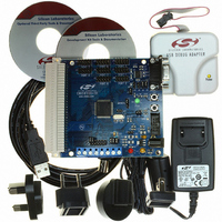
Evaluation Board, Power Supply, USB Cables, Adapter and Documentation
Processor To Be Evaluated
C8051F12x and C8051F13x
Interface Type
USB
Silicon Manufacturer
Silicon Labs
Core Architecture
8051
Silicon Core Number
C8051F120
Silicon Family Name
C8051F12x
Lead Free Status / RoHS Status
Contains lead / RoHS non-compliant
For Use With/related Products
C8051F120, 121, 122, 123, 124, 125, 126, 127
Lead Free Status / Rohs Status
Lead free / RoHS Compliant
Other names
336-1224
Available stocks
Company
Part Number
Manufacturer
Quantity
Price
Company:

Part Number:
C8051F120DK
Manufacturer:
SiliconL
Quantity:
4


13. Reset Sources
14. Oscillators
15. Flash Memory
16. Branch Target Cache
17. External Data Memory Interface and On-Chip XRAM
18. Port Input/Output
19. System Management Bus / I2C Bus (SMBus0)
20. Enhanced Serial Peripheral Interface (SPI0)
Figure 13.1. Reset Sources.................................................................................... 177
Figure 13.2. Reset Timing ...................................................................................... 178
Figure 14.1. Oscillator Diagram.............................................................................. 185
Figure 14.2. PLL Block Diagram............................................................................. 191
Figure 15.1. Flash Memory Map for MOVC Read and MOVX Write Operations ... 201
Figure 15.2. 128 kB Flash Memory Map and Security Bytes ................................. 204
Figure 15.3. 64 kB Flash Memory Map and Security Bytes ................................... 205
Figure 16.1. Branch Target Cache Data Flow ........................................................ 211
Figure 16.2. Branch Target Cache Organiztion...................................................... 212
Figure 16.3. Cache Lock Operation........................................................................ 214
Figure 17.1. Multiplexed Configuration Example.................................................... 222
Figure 17.2. Non-multiplexed Configuration Example ............................................ 223
Figure 17.3. EMIF Operating Modes ...................................................................... 224
Figure 17.4. Non-multiplexed 16-bit MOVX Timing ................................................ 227
Figure 17.5. Non-multiplexed 8-bit MOVX without Bank Select Timing ................. 228
Figure 17.6. Non-multiplexed 8-bit MOVX with Bank Select Timing ...................... 229
Figure 17.7. Multiplexed 16-bit MOVX Timing........................................................ 230
Figure 17.8. Multiplexed 8-bit MOVX without Bank Select Timing ......................... 231
Figure 17.9. Multiplexed 8-bit MOVX with Bank Select Timing .............................. 232
Figure 18.1. Port I/O Cell Block Diagram ............................................................... 235
Figure 18.2. Port I/O Functional Block Diagram ..................................................... 237
Figure 18.3. Priority Crossbar Decode Table (EMIFLE = 0; P1MDIN = 0xFF)....... 238
Figure 18.4. Priority Crossbar Decode Table
Figure 18.5. Priority Crossbar Decode Table
Figure 18.6. Crossbar Example.............................................................................. 244
Figure 19.1. SMBus0 Block Diagram ..................................................................... 259
Figure 19.2. Typical SMBus Configuration ............................................................. 260
Figure 19.3. SMBus Transaction ............................................................................ 261
Figure 19.4. Typical Master Transmitter Sequence................................................ 262
Figure 19.5. Typical Master Receiver Sequence.................................................... 262
Figure 19.6. Typical Slave Transmitter Sequence.................................................. 263
Figure 19.7. Typical Slave Receiver Sequence...................................................... 263
Figure 20.1. SPI Block Diagram ............................................................................. 273
Figure 20.2. Multiple-Master Mode Connection Diagram ....................................... 276
Figure 20.3. 3-Wire Single Master and Slave Mode Connection Diagram ............. 276
(EMIFLE = 1; EMIF in Multiplexed Mode; P1MDIN = 0xFF) ................ 241
(EMIFLE = 1; EMIF in Non-Multiplexed Mode; P1MDIN = 0xFF) ........ 242
Rev. 1.4
C8051F120/1/2/3/4/5/6/7
C8051F130/1/2/3
11
Related parts for C8051F120DK
Image
Part Number
Description
Manufacturer
Datasheet
Request
R

Part Number:
Description:
SMD/C°/SINGLE-ENDED OUTPUT SILICON OSCILLATOR
Manufacturer:
Silicon Laboratories Inc
Part Number:
Description:
Manufacturer:
Silicon Laboratories Inc
Datasheet:
Part Number:
Description:
N/A N/A/SI4010 AES KEYFOB DEMO WITH LCD RX
Manufacturer:
Silicon Laboratories Inc
Datasheet:
Part Number:
Description:
N/A N/A/SI4010 SIMPLIFIED KEY FOB DEMO WITH LED RX
Manufacturer:
Silicon Laboratories Inc
Datasheet:
Part Number:
Description:
N/A/-40 TO 85 OC/EZLINK MODULE; F930/4432 HIGH BAND (REV E/B1)
Manufacturer:
Silicon Laboratories Inc
Part Number:
Description:
EZLink Module; F930/4432 Low Band (rev e/B1)
Manufacturer:
Silicon Laboratories Inc
Part Number:
Description:
I°/4460 10 DBM RADIO TEST CARD 434 MHZ
Manufacturer:
Silicon Laboratories Inc
Part Number:
Description:
I°/4461 14 DBM RADIO TEST CARD 868 MHZ
Manufacturer:
Silicon Laboratories Inc
Part Number:
Description:
I°/4463 20 DBM RFSWITCH RADIO TEST CARD 460 MHZ
Manufacturer:
Silicon Laboratories Inc
Part Number:
Description:
I°/4463 20 DBM RADIO TEST CARD 868 MHZ
Manufacturer:
Silicon Laboratories Inc
Part Number:
Description:
I°/4463 27 DBM RADIO TEST CARD 868 MHZ
Manufacturer:
Silicon Laboratories Inc
Part Number:
Description:
I°/4463 SKYWORKS 30 DBM RADIO TEST CARD 915 MHZ
Manufacturer:
Silicon Laboratories Inc
Part Number:
Description:
N/A N/A/-40 TO 85 OC/4463 RFMD 30 DBM RADIO TEST CARD 915 MHZ
Manufacturer:
Silicon Laboratories Inc
Part Number:
Description:
I°/4463 20 DBM RADIO TEST CARD 169 MHZ
Manufacturer:
Silicon Laboratories Inc