C8051F120DK Silicon Laboratories Inc, C8051F120DK Datasheet - Page 113
C8051F120DK
Manufacturer Part Number
C8051F120DK
Description
DEVKIT-F120/21/22/23/24/25/26/27
Manufacturer
Silicon Laboratories Inc
Type
MCUr
Datasheet
1.C8051F120DK.pdf
(350 pages)
Specifications of C8051F120DK
Contents
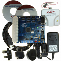
Evaluation Board, Power Supply, USB Cables, Adapter and Documentation
Processor To Be Evaluated
C8051F12x and C8051F13x
Interface Type
USB
Silicon Manufacturer
Silicon Labs
Core Architecture
8051
Silicon Core Number
C8051F120
Silicon Family Name
C8051F12x
Lead Free Status / RoHS Status
Contains lead / RoHS non-compliant
For Use With/related Products
C8051F120, 121, 122, 123, 124, 125, 126, 127
Lead Free Status / Rohs Status
Lead free / RoHS Compliant
Other names
336-1224
Available stocks
Company
Part Number
Manufacturer
Quantity
Price
Company:

Part Number:
C8051F120DK
Manufacturer:
SiliconL
Quantity:
4


C8051F120/1/2/3/4/5/6/7
C8051F130/1/2/3
9.
Voltage Reference
The voltage reference options available on the C8051F12x and C8051F13x device families vary according
to the device capabilities.
All devices include an internal voltage reference circuit, consisting of a 1.2 V, 15 ppm/°C (typical) bandgap
voltage reference generator and a gain-of-two output buffer amplifier. The internal reference may be routed
via the VREF pin to external system components or to the voltage reference input pins. The maximum load
seen by the VREF pin must be less than 200 µA to AGND. Bypass capacitors of 0.1 µF and 4.7 µF are rec-
ommended from the VREF pin to AGND.
The Reference Control Register, REF0CN enables/disables the internal reference generator and the inter-
nal temperature sensor on all devices. The BIASE bit in REF0CN enables the on-board reference genera-
tor while the REFBE bit enables the gain-of-two buffer amplifier which drives the VREF pin. When
disabled, the supply current drawn by the bandgap and buffer amplifier falls to less than 1 µA (typical) and
the output of the buffer amplifier enters a high impedance state. If the internal bandgap is used as the ref-
erence voltage generator, BIASE and REFBE must both be set to logic 1. If the internal reference is not
used, REFBE may be set to logic 0. Note that the BIASE bit must be set to logic 1 if any DACs or ADCs are
used, regardless of whether the voltage reference is derived from the on-chip reference or supplied by an
off-chip source. If no ADCs or DACs are being used, both of these bits can be set to logic 0 to conserve
power.
When enabled, the temperature sensor connects to the highest order input of the ADC0 input multiplexer.
The TEMPE bit within REF0CN enables and disables the temperature sensor. While disabled, the temper-
ature sensor defaults to a high impedance state. Any ADC measurements performed on the sensor while
disabled will result in undefined data.
The electrical specifications for the internal voltage reference are given in Table 9.1.
9.1.
Reference Configuration on the C8051F120/2/4/6
On the C8051F120/2/4/6 devices, the REF0CN register also allows selection of the voltage reference
source for ADC0 and ADC2, as shown in SFR Definition 9.1. Bits AD0VRS and AD2VRS in the REF0CN
register select the ADC0 and ADC2 voltage reference sources, respectively. Three voltage reference input
pins allow each ADC and the two DACs to reference an external voltage reference or the on-chip voltage
reference output (with an external connection). ADC0 may also reference the DAC0 output internally, and
ADC2 may reference the analog power supply voltage, via the VREF multiplexers shown in Figure 9.1.
Rev. 1.4
113
Related parts for C8051F120DK
Image
Part Number
Description
Manufacturer
Datasheet
Request
R

Part Number:
Description:
SMD/C°/SINGLE-ENDED OUTPUT SILICON OSCILLATOR
Manufacturer:
Silicon Laboratories Inc
Part Number:
Description:
Manufacturer:
Silicon Laboratories Inc
Datasheet:
Part Number:
Description:
N/A N/A/SI4010 AES KEYFOB DEMO WITH LCD RX
Manufacturer:
Silicon Laboratories Inc
Datasheet:
Part Number:
Description:
N/A N/A/SI4010 SIMPLIFIED KEY FOB DEMO WITH LED RX
Manufacturer:
Silicon Laboratories Inc
Datasheet:
Part Number:
Description:
N/A/-40 TO 85 OC/EZLINK MODULE; F930/4432 HIGH BAND (REV E/B1)
Manufacturer:
Silicon Laboratories Inc
Part Number:
Description:
EZLink Module; F930/4432 Low Band (rev e/B1)
Manufacturer:
Silicon Laboratories Inc
Part Number:
Description:
I°/4460 10 DBM RADIO TEST CARD 434 MHZ
Manufacturer:
Silicon Laboratories Inc
Part Number:
Description:
I°/4461 14 DBM RADIO TEST CARD 868 MHZ
Manufacturer:
Silicon Laboratories Inc
Part Number:
Description:
I°/4463 20 DBM RFSWITCH RADIO TEST CARD 460 MHZ
Manufacturer:
Silicon Laboratories Inc
Part Number:
Description:
I°/4463 20 DBM RADIO TEST CARD 868 MHZ
Manufacturer:
Silicon Laboratories Inc
Part Number:
Description:
I°/4463 27 DBM RADIO TEST CARD 868 MHZ
Manufacturer:
Silicon Laboratories Inc
Part Number:
Description:
I°/4463 SKYWORKS 30 DBM RADIO TEST CARD 915 MHZ
Manufacturer:
Silicon Laboratories Inc
Part Number:
Description:
N/A N/A/-40 TO 85 OC/4463 RFMD 30 DBM RADIO TEST CARD 915 MHZ
Manufacturer:
Silicon Laboratories Inc
Part Number:
Description:
I°/4463 20 DBM RADIO TEST CARD 169 MHZ
Manufacturer:
Silicon Laboratories Inc