C8051F120DK Silicon Laboratories Inc, C8051F120DK Datasheet - Page 263
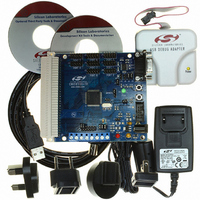
C8051F120DK
Manufacturer Part Number
C8051F120DK
Description
DEVKIT-F120/21/22/23/24/25/26/27
Manufacturer
Silicon Laboratories Inc
Type
MCUr
Datasheet
1.C8051F120DK.pdf
(350 pages)
Specifications of C8051F120DK
Contents
Evaluation Board, Power Supply, USB Cables, Adapter and Documentation
Processor To Be Evaluated
C8051F12x and C8051F13x
Interface Type
USB
Silicon Manufacturer
Silicon Labs
Core Architecture
8051
Silicon Core Number
C8051F120
Silicon Family Name
C8051F12x
Lead Free Status / RoHS Status
Contains lead / RoHS non-compliant
For Use With/related Products
C8051F120, 121, 122, 123, 124, 125, 126, 127
Lead Free Status / Rohs Status
Lead free / RoHS Compliant
Other names
336-1224
Available stocks
Company
Part Number
Manufacturer
Quantity
Price
Company:

Part Number:
C8051F120DK
Manufacturer:
SiliconL
Quantity:
4


19.3.3. Slave Transmitter Mode
Serial data is transmitted on SDA while the serial clock is received on SCL. The SMBus0 interface receives
a START followed by data byte containing the slave address and direction bit. If the received slave address
matches the address held in register SMB0ADR, the SMBus0 interface generates an ACK. SMBus0 will
also ACK if the general call address (0x00) is received and the General Call Address Enable bit
(SMB0ADR.0) is set to logic 1. In this case the data direction bit (R/W) will be logic 1 to indicate a "READ"
operation. The SMBus0 interface receives the clock on SCL and transmits one or more bytes of serial
data, waiting for an ACK from the master after each byte. SMBus0 exits slave mode after receiving a
STOP condition from the master.
19.3.4. Slave Receiver Mode
Serial data is received on SDA while the serial clock is received on SCL. The SMBus0 interface receives a
START followed by data byte containing the slave address and direction bit. If the received slave address
matches the address held in register SMB0ADR, the interface generates an ACK. SMBus0 will also ACK if
the general call address (0x00) is received and the General Call Address Enable bit (SMB0ADR.0) is set to
logic 1. In this case the data direction bit (R/W) will be logic 0 to indicate a "WRITE" operation. The
SMBus0 interface receives one or more bytes of serial data; after each byte is received, the interface
transmits an ACK or NACK depending on the state of the AA bit in SMB0CN. SMBus0 exits Slave Receiver
Mode after receiving a STOP condition from the master.
S
S
Received by SMBus
Interface
Transmitted by
SMBus Interface
Received by SMBus
Interface
Transmitted by
SMBus Interface
Figure 19.6. Typical Slave Transmitter Sequence
Figure 19.7. Typical Slave Receiver Sequence
SLA
SLA
Interrupt
W
R
Interrupt
A
A
Data Byte
Data Byte
Rev. 1.4
C8051F120/1/2/3/4/5/6/7
Interrupt
Interrupt
A
A
S = START
P = STOP
A = ACK
W = WRITE
SLA = Slave Address
S = START
P = STOP
N = NACK
R = READ
SLA = Slave Address
Data Byte
Data Byte
C8051F130/1/2/3
Interrupt
Interrupt
A
N
Interrupt
Interrupt
P
P
263
Related parts for C8051F120DK
Image
Part Number
Description
Manufacturer
Datasheet
Request
R

Part Number:
Description:
SMD/C°/SINGLE-ENDED OUTPUT SILICON OSCILLATOR
Manufacturer:
Silicon Laboratories Inc
Part Number:
Description:
Manufacturer:
Silicon Laboratories Inc
Datasheet:
Part Number:
Description:
N/A N/A/SI4010 AES KEYFOB DEMO WITH LCD RX
Manufacturer:
Silicon Laboratories Inc
Datasheet:
Part Number:
Description:
N/A N/A/SI4010 SIMPLIFIED KEY FOB DEMO WITH LED RX
Manufacturer:
Silicon Laboratories Inc
Datasheet:
Part Number:
Description:
N/A/-40 TO 85 OC/EZLINK MODULE; F930/4432 HIGH BAND (REV E/B1)
Manufacturer:
Silicon Laboratories Inc
Part Number:
Description:
EZLink Module; F930/4432 Low Band (rev e/B1)
Manufacturer:
Silicon Laboratories Inc
Part Number:
Description:
I°/4460 10 DBM RADIO TEST CARD 434 MHZ
Manufacturer:
Silicon Laboratories Inc
Part Number:
Description:
I°/4461 14 DBM RADIO TEST CARD 868 MHZ
Manufacturer:
Silicon Laboratories Inc
Part Number:
Description:
I°/4463 20 DBM RFSWITCH RADIO TEST CARD 460 MHZ
Manufacturer:
Silicon Laboratories Inc
Part Number:
Description:
I°/4463 20 DBM RADIO TEST CARD 868 MHZ
Manufacturer:
Silicon Laboratories Inc
Part Number:
Description:
I°/4463 27 DBM RADIO TEST CARD 868 MHZ
Manufacturer:
Silicon Laboratories Inc
Part Number:
Description:
I°/4463 SKYWORKS 30 DBM RADIO TEST CARD 915 MHZ
Manufacturer:
Silicon Laboratories Inc
Part Number:
Description:
N/A N/A/-40 TO 85 OC/4463 RFMD 30 DBM RADIO TEST CARD 915 MHZ
Manufacturer:
Silicon Laboratories Inc
Part Number:
Description:
I°/4463 20 DBM RADIO TEST CARD 169 MHZ
Manufacturer:
Silicon Laboratories Inc