C8051F120DK Silicon Laboratories Inc, C8051F120DK Datasheet - Page 289
C8051F120DK
Manufacturer Part Number
C8051F120DK
Description
DEVKIT-F120/21/22/23/24/25/26/27
Manufacturer
Silicon Laboratories Inc
Type
MCUr
Datasheet
1.C8051F120DK.pdf
(350 pages)
Specifications of C8051F120DK
Contents
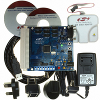
Evaluation Board, Power Supply, USB Cables, Adapter and Documentation
Processor To Be Evaluated
C8051F12x and C8051F13x
Interface Type
USB
Silicon Manufacturer
Silicon Labs
Core Architecture
8051
Silicon Core Number
C8051F120
Silicon Family Name
C8051F12x
Lead Free Status / RoHS Status
Contains lead / RoHS non-compliant
For Use With/related Products
C8051F120, 121, 122, 123, 124, 125, 126, 127
Lead Free Status / Rohs Status
Lead free / RoHS Compliant
Other names
336-1224
Available stocks
Company
Part Number
Manufacturer
Quantity
Price
Company:

Part Number:
C8051F120DK
Manufacturer:
SiliconL
Quantity:
4


21.1.2. Mode 1: 8-Bit UART, Variable Baud Rate
Mode 1 provides standard asynchronous, full duplex communication using a total of 10 bits per data byte:
one start bit, eight data bits (LSB first), and one stop bit. Data are transmitted from the TX0 pin and
received at the RX0 pin. On receive, the eight data bits are stored in SBUF0 and the stop bit goes into
RB80 (SCON0.2).
Data transmission begins when an instruction writes a data byte to the SBUF0 register. The TI0 Transmit
Interrupt Flag (SCON0.1) is set at the end of the transmission (the beginning of the stop-bit time). Data
reception can begin any time after the REN0 Receive Enable bit (SCON0.4) is set to logic 1. After the stop
bit is received, the data byte will be loaded into the SBUF0 receive register if the following conditions are
met: RI0 must be logic 0, and if SM20 is logic 1, the stop bit must be logic 1.
If these conditions are met, the eight bits of data is stored in SBUF0, the stop bit is stored in RB80 and the
RI0 flag is set. If these conditions are not met, SBUF0 and RB80 will not be loaded and the RI0 flag will not
be set. An interrupt will occur if enabled when either TI0 or RI0 are set.
The baud rate generated in Mode 1 is a function of timer overflow. UART0 can use Timer 1 operating in 8-
Bit Auto-Reload Mode , or Timer 2, 3, or 4 operating in Auto-reload Mode to generate the baud rate (note
that the TX and RX clocks are selected separately). On each timer overflow event (a rollover from all ones
- (0xFF for Timer 1, 0xFFFF for Timer 2, 3, or 4) - to zero) a clock is sent to the baud rate logic.
Timers 1, 2, 3, or 4 are selected as the baud rate source with bits in the SSTA0 register (see SFR Defini-
tion 21.2). The transmit baud rate clock is selected using the S0TCLK1 and S0TCLK0 bits, and the receive
baud rate clock is selected using the S0RCLK1 and S0RCLK0 bits.
When Timer 1 is selected as a baud rate source, the SMOD0 bit (SSTA0.4) selects whether or not to divide
the Timer 1 overflow rate by two. On reset, the SMOD0 bit is logic 0, thus selecting the lower speed baud
rate by default. The SMOD0 bit affects the baud rate generated by Timer 1 as shown in Equation 21.1.
The Mode 1 baud rate equations are shown below, where T1M is bit4 of register CKCON, TH1 is the 8-bit
reload register for Timer 1, and [RCAPnH , RCAPnL] is the 16-bit reload register for Timer 2, 3, or 4.
SPACE
MARK
BIT TIMES
BIT SAMPLING
When SMOD0 = 0:
When SMOD0 = 1:
START
BIT
Equation 21.1. Mode 1 Baud Rate using Timer 1
Figure 21.4. UART0 Mode 1 Timing Diagram
D0
Mode1_BaudRate
Mode1_BaudRate
D1
D2
Rev. 1.4
=
=
D3
1 32
1 16
C8051F120/1/2/3/4/5/6/7
D4
Timer1_OverflowRate
Timer1_OverflowRate
D5
C8051F130/1/2/3
D6
D7
STOP
BIT
289
Related parts for C8051F120DK
Image
Part Number
Description
Manufacturer
Datasheet
Request
R

Part Number:
Description:
SMD/C°/SINGLE-ENDED OUTPUT SILICON OSCILLATOR
Manufacturer:
Silicon Laboratories Inc
Part Number:
Description:
Manufacturer:
Silicon Laboratories Inc
Datasheet:
Part Number:
Description:
N/A N/A/SI4010 AES KEYFOB DEMO WITH LCD RX
Manufacturer:
Silicon Laboratories Inc
Datasheet:
Part Number:
Description:
N/A N/A/SI4010 SIMPLIFIED KEY FOB DEMO WITH LED RX
Manufacturer:
Silicon Laboratories Inc
Datasheet:
Part Number:
Description:
N/A/-40 TO 85 OC/EZLINK MODULE; F930/4432 HIGH BAND (REV E/B1)
Manufacturer:
Silicon Laboratories Inc
Part Number:
Description:
EZLink Module; F930/4432 Low Band (rev e/B1)
Manufacturer:
Silicon Laboratories Inc
Part Number:
Description:
I°/4460 10 DBM RADIO TEST CARD 434 MHZ
Manufacturer:
Silicon Laboratories Inc
Part Number:
Description:
I°/4461 14 DBM RADIO TEST CARD 868 MHZ
Manufacturer:
Silicon Laboratories Inc
Part Number:
Description:
I°/4463 20 DBM RFSWITCH RADIO TEST CARD 460 MHZ
Manufacturer:
Silicon Laboratories Inc
Part Number:
Description:
I°/4463 20 DBM RADIO TEST CARD 868 MHZ
Manufacturer:
Silicon Laboratories Inc
Part Number:
Description:
I°/4463 27 DBM RADIO TEST CARD 868 MHZ
Manufacturer:
Silicon Laboratories Inc
Part Number:
Description:
I°/4463 SKYWORKS 30 DBM RADIO TEST CARD 915 MHZ
Manufacturer:
Silicon Laboratories Inc
Part Number:
Description:
N/A N/A/-40 TO 85 OC/4463 RFMD 30 DBM RADIO TEST CARD 915 MHZ
Manufacturer:
Silicon Laboratories Inc
Part Number:
Description:
I°/4463 20 DBM RADIO TEST CARD 169 MHZ
Manufacturer:
Silicon Laboratories Inc