C8051F120DK Silicon Laboratories Inc, C8051F120DK Datasheet - Page 341
C8051F120DK
Manufacturer Part Number
C8051F120DK
Description
DEVKIT-F120/21/22/23/24/25/26/27
Manufacturer
Silicon Laboratories Inc
Type
MCUr
Datasheet
1.C8051F120DK.pdf
(350 pages)
Specifications of C8051F120DK
Contents
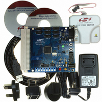
Evaluation Board, Power Supply, USB Cables, Adapter and Documentation
Processor To Be Evaluated
C8051F12x and C8051F13x
Interface Type
USB
Silicon Manufacturer
Silicon Labs
Core Architecture
8051
Silicon Core Number
C8051F120
Silicon Family Name
C8051F12x
Lead Free Status / RoHS Status
Contains lead / RoHS non-compliant
For Use With/related Products
C8051F120, 121, 122, 123, 124, 125, 126, 127
Lead Free Status / Rohs Status
Lead free / RoHS Compliant
Other names
336-1224
Available stocks
Company
Part Number
Manufacturer
Quantity
Price
Company:

Part Number:
C8051F120DK
Manufacturer:
SiliconL
Quantity:
4


25. JTAG (IEEE 1149.1)
Each MCU has an on-chip JTAG interface and logic to support boundary scan for production and in-sys-
tem testing, Flash read/write operations, and non-intrusive in-circuit debug. The JTAG interface is fully
compliant with the IEEE 1149.1 specification. Refer to this specification for detailed descriptions of the Test
Interface and Boundary-Scan Architecture. Access of the JTAG Instruction Register (IR) and Data Regis-
ters (DR) are as described in the Test Access Port and Operation of the IEEE 1149.1 specification.
The JTAG interface is accessed via four dedicated pins on the MCU: TCK, TMS, TDI, and TDO.
Through the 16-bit JTAG Instruction Register (IR), any of the eight instructions shown in Figure 25.1 can
be commanded. There are three DR’s associated with JTAG Boundary-Scan, and four associated with
Flash read/write operations on the MCU.
IR Value
0xFFFF
0x0000
0x0002
0x0004
0x0082
0x0083
0x0084 Flash Address
0x0085
Bit15
Flash Control
JTAG Register Definition 25.1. IR: JTAG Instruction Register
Instruction
Flash Scale
PRELOAD
Flash Data
SAMPLE/
EXTEST
IDCODE
BYPASS
Selects the Boundary Data Register for control and observability of all
device pins
Selects the Boundary Data Register for observability and presetting the
scan-path latches
Selects device ID Register
Selects Bypass Data Register
Selects FLASHCON Register to control how the interface logic responds
to reads and writes to the FLASHDAT Register
Selects FLASHDAT Register for reads and writes to the Flash memory
Selects FLASHADR Register which holds the address of all Flash read,
write, and erase operations
Selects FLASHSCL Register which controls the Flash one-shot timer and
read-always enable
Rev. 1.4
C8051F120/1/2/3/4/5/6/7
Description
C8051F130/1/2/3
Bit0
Reset Value
0x0000
341
Related parts for C8051F120DK
Image
Part Number
Description
Manufacturer
Datasheet
Request
R

Part Number:
Description:
SMD/C°/SINGLE-ENDED OUTPUT SILICON OSCILLATOR
Manufacturer:
Silicon Laboratories Inc
Part Number:
Description:
Manufacturer:
Silicon Laboratories Inc
Datasheet:
Part Number:
Description:
N/A N/A/SI4010 AES KEYFOB DEMO WITH LCD RX
Manufacturer:
Silicon Laboratories Inc
Datasheet:
Part Number:
Description:
N/A N/A/SI4010 SIMPLIFIED KEY FOB DEMO WITH LED RX
Manufacturer:
Silicon Laboratories Inc
Datasheet:
Part Number:
Description:
N/A/-40 TO 85 OC/EZLINK MODULE; F930/4432 HIGH BAND (REV E/B1)
Manufacturer:
Silicon Laboratories Inc
Part Number:
Description:
EZLink Module; F930/4432 Low Band (rev e/B1)
Manufacturer:
Silicon Laboratories Inc
Part Number:
Description:
I°/4460 10 DBM RADIO TEST CARD 434 MHZ
Manufacturer:
Silicon Laboratories Inc
Part Number:
Description:
I°/4461 14 DBM RADIO TEST CARD 868 MHZ
Manufacturer:
Silicon Laboratories Inc
Part Number:
Description:
I°/4463 20 DBM RFSWITCH RADIO TEST CARD 460 MHZ
Manufacturer:
Silicon Laboratories Inc
Part Number:
Description:
I°/4463 20 DBM RADIO TEST CARD 868 MHZ
Manufacturer:
Silicon Laboratories Inc
Part Number:
Description:
I°/4463 27 DBM RADIO TEST CARD 868 MHZ
Manufacturer:
Silicon Laboratories Inc
Part Number:
Description:
I°/4463 SKYWORKS 30 DBM RADIO TEST CARD 915 MHZ
Manufacturer:
Silicon Laboratories Inc
Part Number:
Description:
N/A N/A/-40 TO 85 OC/4463 RFMD 30 DBM RADIO TEST CARD 915 MHZ
Manufacturer:
Silicon Laboratories Inc
Part Number:
Description:
I°/4463 20 DBM RADIO TEST CARD 169 MHZ
Manufacturer:
Silicon Laboratories Inc