C8051F310DK Silicon Laboratories Inc, C8051F310DK Datasheet - Page 8
C8051F310DK
Manufacturer Part Number
C8051F310DK
Description
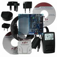
DEV KIT FOR C8051F310/F311
Manufacturer
Silicon Laboratories Inc
Type
MCUr
Specifications of C8051F310DK
Contents
Evaluation Board, Power Supply, USB Cables, Adapter and Documentation
Processor To Be Evaluated
C8051F31x
Interface Type
USB
Silicon Manufacturer
Silicon Labs
Core Architecture
8051
Silicon Core Number
C8051F310
Silicon Family Name
C8051F31x
Lead Free Status / RoHS Status
Contains lead / RoHS non-compliant
For Use With/related Products
Silicon Laboratories C8051, F310, 311 MCUs
Lead Free Status / Rohs Status
Lead free / RoHS Compliant
Other names
336-1253
Available stocks
Company
Part Number
Manufacturer
Quantity
Price
Company:

Part Number:
C8051F310DK
Manufacturer:
SiliconL
Quantity:
10


C8051F31x-DK
6.5. Serial Interface (J5)
A RS232 transceiver circuit and DB-9 (J5) connector are provided on the target board to facilitate serial connec-
tions to UART0 of the C8051F310. The TX, RX, RTS and CTS signals of UART0 may be connected to the DB-9
connector and transceiver by installing shorting blocks on header J3.
6.6. Analog I/O (J6)
Several of the C8051F310 target device’s port pins are connected to the J6 terminal block. Refer to Table 4 for the
J6 terminal block connections. Install a shorting block on J7[2-3] to connect the AIN2.4 input to the P2.4 pin of the
target device.
6.7. USB Debug Adapter Target Board Power Connector (J8)
The USB Debug Adapter includes a connection to provide power to the target board. This connection is routed
from J4[10] to J8[1]. Place a shorting block at header J8[2–3] to power the board directly from an ac/dc power
adapter. Place a shorting block at header J8[1–2] to power the board from the USB Debug Adapter. Please note
that the second option is not supported with either the EC1 or EC2 Serial Adapters.
6.8. Low-pass Filter (J7)
The C8051F310 target board features a low-pass filter that may be connected to port pin P2.4. Install a shorting
block on J7[1–2] to connect the P2.4 pin of the target device to the low-pass filter input. The output of the low-pass
filter is routed to the PWM signal at J1[2]. The C8051F310 may be programmed to generate a PWM (Pulse-Width
Modulated) waveform which is then input to the low-pass filter to implement a user-controlled PWM digital-to-ana-
log converter. Refer to Applications Note “AN107: Implementing 16-Bit PWM Using the PCA” in the “documenta-
tion” directory on the CD-ROM for a discussion on generating a programmable dc voltage level with a PWM
waveform and low-pass filter.
8
J3[5–6]
J3[7–8]
J3[9–10] - Install shorting block to connect UART0 RTS (P3.1) to transceiver.
J3[11–12] - Install shorting block to connect UART0 CTS (P3.2) to transceiver.
- Install shorting block to connect UART0 TX (P0.4) to transceiver.
- Install shorting block to connect UART0 RX (P0.5) to transceiver.
Table 4. J6 Terminal Block Pin Descriptions
Pin #
1
2
3
4
P0.0 / Vref (Voltage Reference)
Rev. 0.6
GND (Ground)
Description
P2.5 / AIN2.5
AIN2.4
Related parts for C8051F310DK
Image
Part Number
Description
Manufacturer
Datasheet
Request
R

Part Number:
Description:
SMD/C°/SINGLE-ENDED OUTPUT SILICON OSCILLATOR
Manufacturer:
Silicon Laboratories Inc
Part Number:
Description:
Manufacturer:
Silicon Laboratories Inc
Datasheet:
Part Number:
Description:
N/A N/A/SI4010 AES KEYFOB DEMO WITH LCD RX
Manufacturer:
Silicon Laboratories Inc
Datasheet:
Part Number:
Description:
N/A N/A/SI4010 SIMPLIFIED KEY FOB DEMO WITH LED RX
Manufacturer:
Silicon Laboratories Inc
Datasheet:
Part Number:
Description:
N/A/-40 TO 85 OC/EZLINK MODULE; F930/4432 HIGH BAND (REV E/B1)
Manufacturer:
Silicon Laboratories Inc
Part Number:
Description:
EZLink Module; F930/4432 Low Band (rev e/B1)
Manufacturer:
Silicon Laboratories Inc
Part Number:
Description:
I°/4460 10 DBM RADIO TEST CARD 434 MHZ
Manufacturer:
Silicon Laboratories Inc
Part Number:
Description:
I°/4461 14 DBM RADIO TEST CARD 868 MHZ
Manufacturer:
Silicon Laboratories Inc
Part Number:
Description:
I°/4463 20 DBM RFSWITCH RADIO TEST CARD 460 MHZ
Manufacturer:
Silicon Laboratories Inc
Part Number:
Description:
I°/4463 20 DBM RADIO TEST CARD 868 MHZ
Manufacturer:
Silicon Laboratories Inc
Part Number:
Description:
I°/4463 27 DBM RADIO TEST CARD 868 MHZ
Manufacturer:
Silicon Laboratories Inc
Part Number:
Description:
I°/4463 SKYWORKS 30 DBM RADIO TEST CARD 915 MHZ
Manufacturer:
Silicon Laboratories Inc
Part Number:
Description:
N/A N/A/-40 TO 85 OC/4463 RFMD 30 DBM RADIO TEST CARD 915 MHZ
Manufacturer:
Silicon Laboratories Inc
Part Number:
Description:
I°/4463 20 DBM RADIO TEST CARD 169 MHZ
Manufacturer:
Silicon Laboratories Inc