C8051F226DK Silicon Laboratories Inc, C8051F226DK Datasheet
C8051F226DK
Specifications of C8051F226DK


Related parts for C8051F226DK

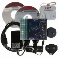
C8051F226DK Summary of contents
Page 1
Analog Peripherals - SAR ADC 12-bit resolution ('F206) • 8-bit resolution ('F220/1/6) • ±1/4 LSB INL (8-bit) and ±2 LSB INL (12-bit) • 100 ksps • channel input multiplexer; each port • I/O pin can ...
Page 2
C8051F2xx N : OTES 2 Rev. 1.6 ...
Page 3
Table of Contents 1. System Overview.................................................................................................... 11 1.1. CIP-51TM Microcontroller Core ........................................................................ 15 1.1.1. Fully 8051 Compatible.............................................................................. 15 1.1.2. Improved Throughput ............................................................................... 15 1.1.3. Additional Features .................................................................................. 16 1.2. On-Board Memory ............................................................................................ 17 1.3. JTAG ............................................................................................................ 18 1.4. Digital/Analog Configurable ...
Page 4
C8051F2xx 9.5. Power Management Modes .............................................................................. 83 9.5.1. Idle Mode.................................................................................................. 83 9.5.2. Stop Mode ................................................................................................ 83 10. Flash Memory ......................................................................................................... 85 10.1.Programming The Flash Memory ..................................................................... 85 10.2.Security Options ............................................................................................... 86 11. On-Chip XRAM (C8051F206/226/236).................................................................... 90 12. Reset Sources......................................................................................................... 91 ...
Page 5
Counter/Timer with Capture ........................................... 134 17.2.2.Mode 1: 16-bit Counter/Timer with Auto-Reload.................................... 135 17.2.3.Mode 2: Baud Rate Generator ............................................................... 136 18. JTAG ...................................................................................................................... 139 18.1.Flash Programming Commands..................................................................... 140 18.2.Boundary Scan Bypass and ID Code ...
Page 6
C8051F2xx N : OTES 6 Rev. 1.6 ...
Page 7
List of Figures and Tables 1. System Overview Table 1.1. Product Selection Guide ........................................................................ 11 Figure 1.1. C8051F206, C8051F220 and C8051F226 Block Diagram (48 TQFP Figure 1.2. C8051F221 Block Diagram (32 LQFP) .................................................. 13 Figure 1.3. C8051F230 and ...
Page 8
C8051F2xx Table 9.1. CIP-51 Instruction Set Summary............................................................ 60 Figure 9.2. Memory Map .......................................................................................... 66 Table 9.2. Special Function Register Memory Map ................................................ 68 Table 9.3. Special Function Registers .................................................................... 69 Table 9.4. Interrupt Summary ................................................................................. 75 10. Flash Memory Table ...
Page 9
List of Registers SFR Definition 5.1. AMX0SL: AMUX Channel Select . . . . . . . . . . . . . . . . . . . . . . . . . . 34 SFR Definition 5.2. ...
Page 10
C8051F2xx SFR Definition 14.4. P0: Port0 Register . . . . . . . . . . . . . . . . . . . . . . . . . . . . . . . . . ...
Page 11
System Overview The C8051F2xx is a family of fully integrated, mixed-signal System on a Chip MCU's available with a true 12-bit ('F206) multi-channel ADC, 8-bit multi-channel ADC ('F220/1/6 and 'F206), or without an ADC ('F230/1/6). Each model features an ...
Page 12
C8051F2xx Digital Power VDD VDD GND GND TCK JTAG TMS Emulation HW TDI Logic TDO /RST VDD Monitor, VDDMONEN WDT External XTAL1 Oscillator XTAL2 Circuit System Clock Internal Oscillator Figure 1.1. C8051F206, C8051F220 and C8051F226 Block Diagram ...
Page 13
Digital Power VDD GND TCK 8 JTAG TMS Emulation HW Logic TDI 0 TDO 5 Reset /RST 1 VDD Monitor, WDT C External o XTAL1 Oscillator XTAL2 r Circuit System Clock e Internal Oscillator Figure 1.2. C8051F221 Block Diagram (32 ...
Page 14
C8051F2xx Digital Power VDD GND GND TCK JTAG TMS Emulation HW TDI Logic TDO /RST VDD Monitor, MONEN WDT External XTAL1 Oscillator XTAL2 Circuit System Clock Internal NC Oscillator Figure 1.3. C8051F230 and C8051F236 Block Diagram ...
Page 15
Digital Power VDD GND TCK JTAG TMS Emulation HW TDI Logic TDO Reset /RST VDD Monitor, WDT External XTAL1 Oscillator XTAL2 Circuit System Clock Internal Oscillator NC Figure 1.4. C8051F231 Block Diagram (32 LQFP) TM 1.1. CIP-51 Microcontroller Core 1.1.1. ...
Page 16
C8051F2xx With the CIP-51's maximum system clock at 25 MHz, it has a peak throughput of 25 MIPS. Figure 1.5 shows a comparison of peak throughputs of various 8-bit microcontroller cores with their maximum system clocks ...
Page 17
Comparator 0 CP0 CP0- C0RSEF Missing System Clock Clock Detector EN Figure 1.6. Comparison of Peak MCU Throughputs 1.2. On-Board Memory The CIP-51 has a standard 8051 program and data address configuration. It includes 256 bytes of data ...
Page 18
C8051F2xx PROGRAM MEMORY 0x207F 128 Byte ISP FLASH 0x2000 0x1FFF RESERVED 0x1E00 0x1DFF FLASH (In-System Programmable in 512 Byte Sectors) 0x0000 Figure 1.7. On-Board Memory Map 1.3. JTAG The C8051F2xx have on-chip JTAG and debug logic that provide non-intrusive, full ...
Page 19
WINDOWS OS Figure 1.8. Degub Environment Diagram 1.4. Digital/Analog Configurable I/O The standard 8051 Ports ( and 3) are available on the device. The ports behave like standard 8051 ports with a few enhancements. Each port pin can ...
Page 20
C8051F2xx T0,T1,T2 Timers UART External INT0 & INT1 Comparators 0 & 1 SYSCLK SPI A ADC Figure 1.9. Port I/O Functional Block Diagram 1.5. Serial Ports The C8051F206, C8051F220/1/6 and C8051F230/1/6 include a Full-Duplex UART and SPI ...
Page 21
ADC data is continuously monitored by a programmable window detector, which interrupts the CPU when data is within the user-programmed window. This allows the ADC to monitor key system voltages in back- ground mode, without the use of CPU resources. ...
Page 22
C8051F2xx CP0 P1.2 CP1 P1.5 P1.0 + CP0 - P1.1 P1.3 + CP1 - P1.4 Figure 1.11. Comparator Diagram 22 Port1 MUX CP0 SFR's CP1 (Data and Cntrl) Rev. 1.6 CIP-51 and Interrupt Handler ...
Page 23
Absolute Maximum Ratings Table 2.1. Absolute Maximum Ratings Parameter Ambient Temperature under Bias Storage Temperature Voltage on any Pin (except V and Port I/O) with DD respect to DGND Voltage on any Port I/O Pin or RST pins with ...
Page 24
C8051F2xx 3. Global DC Electrical Characteristics Table 3.1. Global DC Electrical Characteristics –40 to +85 °C unless otherwise specified. Parameter 1 Analog Supply Voltage V supply current with ADC and DD comparators active, and CPU active V supply current with ...
Page 25
Pinout and Package Definitions ‘F206, F220, ‘F221, 226, 231 Name Type 230, 236 48-Pin 32-Pin V 11, GND 5,6,8, 9 13,32 MONEN TCK TMS TDI 28 ...
Page 26
C8051F2xx Table 4.1. Pin Definitions (Continued) ‘F206, F220, ‘F221, 226, 231 Name Type 230, 236 48-Pin 32-Pin P0.3/INT1 I P0.4/ I P0.5/ I P0.6/T2 34 ...
Page 27
Table 4.1. Pin Definitions (Continued) ‘F206, F220, ‘F221, 226, 231 Name Type 230, 236 48-Pin 32-Pin ...
Page 28
C8051F2xx P1.3/CP1+ 1 P1.2/CP0 2 P1.1/CP0- 3 P1.0/CP0 VREF XTAL1 XTAL2 10 VDD 11 MONEN 12 Figure 4.1. TQFP-48 Pin Diagram 28 C8051F220/6 C8051F230/6 C8051F206 *Pin Connect ...
Page 29
P1.3/CP1 P1.2/CP0 3 P1.1/CP0- C8051F221 4 P1.0/CP0+ C8051F231 VREF* 5 XTAL1 6 7 XTAL2 8 VDD *Pin Connect Figure 4.2. LQFP-32 Pin Diagram C8051F2xx (NC) on 'F231 Rev. 1.6 24 P0.4/T0 23 P0.5/T1 22 ...
Page 30
C8051F2xx PIN 1 IDENTIFIER Figure 4.3. TQFP-48 Package Drawing Rev. 1.6 MIN NOM MAX (mm) (mm) (mm ...
Page 31
PIN 1 IDENTIFIER Figure 4.4. LQFP-32 Package Drawing C8051F2xx MIN (mm 0. 1. Rev. 1.6 NOM MAX (mm) (mm) ...
Page 32
C8051F2xx 5. ADC (8-Bit, C8051F220/1/6 Only) Description The ADC subsystem for the C8051F220/1/6 consists of configurable analog multiplexer (AMUX), a pro- grammable gain amplifier (PGA), and a 100ksps, 8-bit successive-approximation-register ADC with inte- grated track-and-hold and programmable window detector (see ...
Page 33
ADC Modes of Operation The ADC has a maximum conversion speed of 100ksps. The ADC conversion clock is derived from the system clock. The ADC conversion clock is derived from a divided version of SYSCLK. Divide ratios of 1,2,4,8, ...
Page 34
C8051F2xx SFR Definition 5.1. AMX0SL: AMUX Channel Select R/W R/W R AMXEN Bit7 Bit6 Bit5 Bits 7–6: UNUSED. Read = 00b; Write = don't care Bit 5: AMXEN enable 0: AMXEN disabled and port pins are unavailable for ...
Page 35
SFR Definition 5.2. ADC0CF: ADC Configuration Register R/W R/W R/W ADCSC2 ADCSC1 ADCSC0 Bit7 Bit6 Bit5 Bits7–5: ADCSC2–0: ADC SAR Conversion Clock Period Bits 000: SAR Conversion Clock = 1 System Clock 001: SAR Conversion Clock = 2 System Clocks ...
Page 36
C8051F2xx SFR Definition 5.3. ADC0CN: ADC Control (C8051F220/1/6 and C8051F206) R/W R/W R/W ADCEN ADCTM ADCINT ADBUSY ADSTM1 ADSTM0 ADWINT Bit7 Bit6 Bit5 Bit7: ADCEN: ADC Enable Bit 0: ADC Disabled. ADC is in low power shutdown. 1: ADC Enabled. ...
Page 37
SFR Definition 5.4. ADC0H: ADC Data Word (‘F220/1/6 and ‘F206) R/W R/W R/W MSB Bit7 Bit6 Bit5 Bits7–0: ADC Data Word Bits EXAMPLE : ADC Data Word Conversion Map AIN – GND(Volts) REF x (255/256) REF x ½ REF x ...
Page 38
C8051F2xx Input Voltage ADC Data (Analog Input - GND) Word REF x (255/256) 0xFF 0x21 REF x (32/256) 0x20 ADC0LTH 0x1F 0x11 REF x (16/256) 0x10 ADC0GTH 0x0F 0x00 0 Given: AMX0SL = 0x00, AMX0CF = 0x00, ADLJST = 0, ...
Page 39
Table 5.1. 8-Bit ADC Electrical Characteristics VDD = 3.0 V, VREF = 2.40 V, PGA Gain = 1, –40 to +85 ×C unless otherwise specified. Parameter DC Accuracy Resolution Integral Nonlinearity Differential Nonlinearity Offset Error Gain Error Offset Temperature Coefficient ...
Page 40
C8051F2xx 6. ADC (12-Bit, C8051F206 Only) Description The ADC subsystem for the C8051F206 consists of configurable analog multiplexer (AMUX), a program- mable gain amplifier (PGA), and a 100ksps, 12-bit successive-approximation-register ADC with integrated track-and-hold and programmable window detector (see Figure ...
Page 41
ADC Modes of Operation The ADC has a maximum conversion speed of 100 ksps. The ADC conversion clock is derived from the system clock. The ADC conversion clock is derived from a divided version of SYSCLK. Divide ratios of ...
Page 42
C8051F2xx SFR Definition 6.1. AMX0SL: AMUX Channel Select R/W R/W R AMXEN Bit7 Bit6 Bit5 Bits 7–6: UNUSED. Read = 00b; Write = don’t care Bit 5: AMXEN enable 0: AMXEN disabled and port pins are unavailable for ...
Page 43
SFR Definition 6.2. ADC0CF: ADC Configuration (‘F220/1/6 and ‘F206) R/W R/W R/W ADCSC2 ADCSC1 ADCSC0 Bit7 Bit6 Bit5 Bits7–5: ADCSC2–0: ADC SAR Conversion Clock Period Bits 000: SAR Conversion Clock = 1 System Clock 001: SAR Conversion Clock = 2 ...
Page 44
C8051F2xx SFR Definition 6.3. ADC0CN: ADC Control (‘F220/1/6 and ‘F206) R/W R/W R/W ADCEN ADCTM ADCINT ADBUSY ADSTM1 ADSTM0 ADWINT Bit7 Bit6 Bit5 Bit7: ADCEN: ADC Enable Bit 0: ADC Disabled. ADC is in low power shutdown. 1: ADC Enabled. ...
Page 45
SFR Definition 6.4. ADC0H: ADC Data Word MSB (C8051F206) R/W R/W R/W Bit7 Bit6 Bit5 Bits7–0: ADC Data Word Bits For ADLJST = 1: Upper 8-bits of the 12-bit ADC Data Word. For ADLJST = 0: Bits7–4 are the sign ...
Page 46
C8051F2xx 6.3. ADC Programmable Window Detector The ADC programmable window detector is very useful in many applications. It continuously compares the ADC output to user-programmed limits and notifies the system when an out-of-band condition is detected. This is especially effective ...
Page 47
SFR Definition 6.9. ADC0LTL: ADC Less-Than Data Low Byte (C8051F206) R/W R/W R/W Bit7 Bit6 Bit5 Bits7–0: These bits are the low byte of the ADC Less-Than Data Word. Definition: ADC Less-Than Data Word = ADC0LTH:ADC0LTL Input Voltage ADC Data ...
Page 48
C8051F2xx Input Voltage ADC Data (AD0 - AGND) Word REF x (4095/4096) 0xFFF0 ADWINT not affected 0x2010 REF x (512/4096) 0x2000 ADC0LTH:ADC0LTL 0x1FF0 ADWINT=1 0x1010 REF x (256/4096) 0x1000 ADC0GTH:ADC0GTL 0x0FF0 ADWINT not affected 0x0000 0 Given: AMX0SL = 0x00, ...
Page 49
Table 6.1. 12-Bit ADC Electrical Characteristics (C8015F206 only 3.0 V, VREF = 2.40 V (REFBE=0), PGA Gain = 1, –40 to +85 °C unless otherwise specified. DD Parameter DC Accuracy Resolution Integral Nonlinearity Differential Nonlinearity Offset Error Full ...
Page 50
C8051F2xx 7. Voltage Reference (C8051F206/220/221/226) The voltage reference circuit selects between an externally connected reference and the power supply voltage (V ). (See Figure 7.1 external reference can be connected to the VREF pin and selected by setting ...
Page 51
Table 7.1. Reference Electrical Characteristics V = 3.0 V, Temperature –40 to +85 ×C DD External Reference ([REFSL1: REFSL0] = 00), V Input Voltage Range Input Current Input Resistance C8051F2xx = 2.4 V) Min Typ REF (V 1.00 — — ...
Page 52
C8051F2xx 8. Comparators The MCU has two on-board voltage comparators as shown in Figure 8.1. The inputs of each Comparator are available at the package pins. The output of each comparator is optionally available at port1 by config- uring (see ...
Page 53
CP0EN CP0OUT CP0RIF CP0FIF CP0HYP1 CP0HYP0 CP0HYN1 CP0HYN0 P1.0/CP0+ P1.1/CP0- CP1EN CP1OUT CP1RIF CP1FIF CP1HYP1 CP1HYP0 CP1HYN1 CP1HYN0 P1.3/CP1+ P1.4/CP1- Figure 8.1. Comparator Functional Block Diagram C8051F2xx AV+ Reset Decision Tree + Synchronizer - AGND AV+ + Synchronizer - AGND ...
Page 54
C8051F2xx CP0+ VIN+ + CP0 CP0- _ VIN- CIRCUIT CONFIGURATION Positive Hysteresis Voltage (Programmed with CP0HYSP Bits) VIN- INPUTS VIN OUTPUT V OL Positive Hysteresis Disabled Figure 8.2. Comparator Hysteresis Plot 54 OUT Negative Hysteresis Voltage (Programmed by ...
Page 55
SFR Definition 8.1. CPT0CN: Comparator 0 Control R/W R R/W CP0EN CP0OUT CP0RIF Bit7 Bit6 Bit5 Bit7: CP0EN: Comparator 0 Enable Bit 0: Comparator 0 Disabled. 1: Comparator 0 Enabled. Bit6: CP0OUT: Comparator 0 Output State Flag 0: Voltage on ...
Page 56
C8051F2xx SFR Definition 8.2. CPT1CN: Comparator 1 Control R/W R R/W CP1EN CP1OUT CP1RIF Bit7 Bit6 Bit5 Bit7: CP1EN: Comparator 1 Enable Bit 0: Comparator 1 Disabled. 1: Comparator 1 Enabled. Bit6: CP1OUT: Comparator 1 Output State Flag 0: Voltage ...
Page 57
Table 8.1. Comparator Electrical Characteristics V = 3.0 V, –40 to +85 ×C unless otherwise specified. DD Parameter Response Time1* (CP+) – (CP–) = 100 mV Response Time2* (CP+) – (CP– Common Mode Rejection Ratio Positive Hysteresis1 ...
Page 58
C8051F2xx 9. CIP-51 Microcontroller General Description The MCU’s system controller core is the CIP-51 microcontroller. The CIP-51 is fully compatible with the TM MCS-51 instruction set. Standard 803x/805x assemblers and compilers can be used to develop soft- ware. The MCU ...
Page 59
Performance The CIP-51 employs a pipelined architecture that greatly increases its instruction throughput over the stan- dard 8051 architecture standard 8051, all instructions except for MUL and DIV take system clock cycles to execute, and ...
Page 60
C8051F2xx 9.1. Instruction Set The instruction set of the CIP-51 System Controller is fully compatible with the standard MCS-51™ instruc- tion set. Standard 8051 development tools can be used to develop software for the CIP-51. All CIP-51 instructions are the ...
Page 61
Table 9.1. CIP-51 Instruction Set Summary (Continued) Mnemonic INC @Ri Increment indirect RAM DEC A Decrement A DEC Rn Decrement register DEC direct Decrement direct byte DEC @Ri Decrement indirect RAM INC DPTR Increment Data Pointer MUL AB Multiply A ...
Page 62
C8051F2xx Table 9.1. CIP-51 Instruction Set Summary (Continued) Mnemonic MOV A,#data Move immediate to A MOV Rn,A Move A to register MOV Rn,direct Move direct byte to register MOV Rn,#data Move immediate to register MOV direct,A Move A to direct ...
Page 63
Table 9.1. CIP-51 Instruction Set Summary (Continued) Mnemonic JNC rel Jump if carry not set JB bit,rel Jump if direct bit is set JNB bit,rel Jump if direct bit is not set JBC bit,rel Jump if direct bit is set ...
Page 64
C8051F2xx Notes on Registers, Operands and Addressing Modes Register R0–R7 of the currently selected register bank. @Ri - Data RAM location addressed indirectly through register R0–R1 rel - 8-bit, signed (two’s compliment) offset relative to the first byte ...
Page 65
Memory Organization The memory organization of the CIP-51 System Controller is similar to that of a standard 8051. There are two separate memory spaces: program memory and data memory. Program and data memory share the same address space but ...
Page 66
C8051F2xx PROGRAM MEMORY 0x207F 128 Byte ISP FLASH 0x2000 0x1FFF RESERVED 0x1E00 0x1DFF FLASH (In-System Programmable in 512 Byte Sectors) 0x0000 9.2.3. General Purpose Registers The lower 32 bytes of data memory, locations 0x00 through 0x1F, may be addressed as ...
Page 67
Stack A programmer's stack can be located anywhere in the 256-byte data memory. The stack area is desig- nated using the Stack Pointer (SP, 0x81) SFR. The SP will point to the last location used. The next value pushed ...
Page 68
C8051F2xx 9.3. Special Function Registers The direct-access data memory locations from 0x80 to 0xFF constitute the special function registers (SFRs). The SFRs provide control and data exchange with the CIP-51's resources and peripherals. The CIP-51 duplicates the SFRs found in ...
Page 69
Table 9.3. Special Function Registers SFR’s are listed in alphabetical order. Address Register 0xE0 ACC 0xBC ADC0CF 0xE8 ADC0CN 0xC5 ADC0GTH 0xC4 ADC0GTL 0xBF ADC0H 0xBE ADC0L 0xC7 ADC0LTH 0xCE ADC0LTL 0xBB AMX0SL 0xF0 B 0x8E CKCON 0x9E CPT0CN 0x9F ...
Page 70
C8051F2xx Table 9.3. Special Function Registers (Continued) SFR’s are listed in alphabetical order. Address Register 0xA4 PRT0CF 0xA5 PRT1CF 0xA6 PRT2CF 0xA7 PRT3CF 0xE1 PRT0MX 0xE2 PRT1MX 0xE3 PRT2MX 0x8F PSCTL 0xD0 PSW 0xCB RCAP2H 0xCA RCAP2L 0xD1 REF0CN 0xEF ...
Page 71
Register Descriptions Following are descriptions of SFRs related to the operation of the CIP-51 System Controller. Reserved bits should be set to logic 0. Future product versions may use these bits to implement new features in which case the ...
Page 72
C8051F2xx SFR Definition 9.4. PSW: Program Status Word R/W R/W R Bit7 Bit6 Bit5 CY: Carry Flag. Bit7: This bit is set when the last arithmetic operation results in a carry (addition borrow (subtraction). ...
Page 73
SFR Definition 9.5. ACC: Accumulator R/W R/W R/W ACC.7 ACC.6 ACC.5 ACC.4 Bit7 Bit6 Bit5 Bits 7–0: ACC: Accumulator This register is the accumulator for arithmetic operations. SFR Definition 9. Register R/W R/W R/W B.7 B.6 B.5 Bit7 ...
Page 74
C8051F2xx 9.4. Interrupt Handler The CIP-51 includes an extended interrupt system supporting interrupt sources with two priority levels. The allocation of interrupt sources between on-chip peripherals and external inputs pins varies according to the specific version of ...
Page 75
SFR Definition 9.7. SWCINT: Software Controlled Interrupt Register R/W R/W R/W SCI3 SCI2 SCI1 Bit7 Bit6 Bit5 Bit7: SCI3: Software Controlled Interrupt 3 Bit. If enabled, writing a logic 1 to this interrupt control bit will cause the CPU to ...
Page 76
C8051F2xx Table 9.4. Interrupt Summary (Continued) Interrupt Interrupt Source Vector ADC0 End of Conversion 0x007B Software Controlled Interrupt 0 0x0083 Software Controlled Interrupt 1 0x008B Software Controlled Interrupt 2 0x0093 Software Controlled Interrupt 3 0x009B Unused Interrupt Location 0x00A3 External ...
Page 77
Interrupt Register Descriptions The SFRs used to enable the interrupt sources and set their priority level are described below. Refer to the datasheet section associated with a particular on-chip peripheral for information regarding valid inter- rupt conditions for the ...
Page 78
C8051F2xx SFR Definition 9.9. IP: Interrupt Priority R/W R/W R PT2 Bit7 Bit6 Bit5 Bits7–6: UNUSED. Read = 00b, Write = don't care. Bit5: PT2 Timer 2 Interrupt Priority Control. This bit sets the priority of the Timer ...
Page 79
SFR Definition 9.10. EIE1: Extended Interrupt Enable 1 R/W R/W R/W ECP1R ECP1F ECP0R Bit7 Bit6 Bit5 Bit7: ECP1R: Enable Comparator 1 (CP1) Rising Edge Interrupt. This bit sets the masking of the CP1 interrupt. 0: Disable CP1 Rising Edge ...
Page 80
C8051F2xx SFR Definition 9.11. EIE2: Extended Interrupt Enable 2 R/W R/W R/W EXVLD - ESCI3 Bit7 Bit6 Bit5 Bit7: EXVLD: Enable External Clock Source Valid (XTLVLD) Interrupt. This bit sets the masking of the XTLVLD interrupt. 0: Disable all XTLVLD ...
Page 81
SFR Definition 9.12. EIP1: Extended Interrupt Priority 1 R/W R/W R/W PCP1R PCP1F PCP0R Bit7 Bit6 Bit5 Bit7: PCP1R: Comparator 1 (CP1) Rising Interrupt Priority Control. This bit sets the priority of the CP1 interrupt. 0: CP1 rising interrupt set ...
Page 82
C8051F2xx SFR Definition 9.13. EIP2: Extended Interrupt Priority 2 R/W R/W R/W PXVLD - PSCI3 Bit7 Bit6 Bit5 Bit7: PXVLD: External Clock Source Valid (XTLVLD) Interrupt Priority Control. This bit sets the priority of the XTLVLD interrupt. 0: XTLVLD interrupt ...
Page 83
Power Management Modes The CIP-51 core has two software programmable power management modes: Idle and Stop. Idle mode halts the CPU while leaving the external peripherals and internal clocks active. In Stop mode, the CPU is halted, all interrupts ...
Page 84
C8051F2xx down all digital peripherals. Each analog peripheral must be shut down individually prior to entering Stop Mode. Stop mode can only be terminated by an internal or external reset. On reset, the CIP-51 performs the normal reset sequence and ...
Page 85
Flash Memory This MCU includes 128 bytes of on-chip, re-programmable Flash memory for program code and non- volatile data storage. The Flash memory can be programmed in-system, a single byte at a time, through the JTAG ...
Page 86
C8051F2xx write/erase operations are disabled. Note that code execution in the 8051 is stalled while the Flash is being programmed or erased. Table 10.1. Flash Memory Electrical Characteristics V = 2.7 to 3.6 V, –40 to +85 ×C unless otherwise ...
Page 87
Block locked only if all other blocks are locked) Read Lock Byte Write/Erase Lock Byte Program Memory Space Software Read Limit Flash Read Lock Byte Bits7–0: Each bit locks a corresponding block of memory. (Bit 7 is MSB.) 0: ...
Page 88
C8051F2xx The Flash Access Limit security feature protects proprietary program code and data from being read by software running on the CIP-51. This feature provides support for OEMs that wish to program the MCU with proprietary value-added firmware before distribution. ...
Page 89
SFR Definition 10.2. FLSCL: Flash Memory Timing Prescaler R/W R/W R/W FOSE FRAE - Bit7 Bit6 Bit5 Bit7: FOSE: Flash One-Shot Timer Enable 0: Flash One-shot timer disabled. 1: Flash One-shot timer enabled Bit6: FRAE: Flash Read Always Enable 0: ...
Page 90
C8051F2xx 11. On-Chip XRAM (C8051F206/226/236) The C8051F206/226/236 features 1024 Bytes of RAM mapped into the external data memory space. All address locations may be accessed using the external move instruction (MOVX) and the data pointer (DPTR), or using indirect MOVX ...
Page 91
Reset Sources The reset circuitry of the MCU allows the controller to be easily placed in a predefined default condition. On entry to this reset state, the CIP-51 halts program execution, forces the external port pins to a known ...
Page 92
C8051F2xx 12.1. Power-on Reset The CIP-51 incorporates a power supply monitor that holds the MCU in the reset state until V above the VRST level during power-up. (See Figure 12.2 for timing diagram, and refer to Table 12.1 for the ...
Page 93
External Reset The external RST pin provides a means for external circuitry to force the CIP-51 into a reset state. Assert- ing an active-low signal on the RST pin will cause the CIP-51 to enter the reset state. Although ...
Page 94
C8051F2xx Disable WDT Writing 0xDE followed by 0xAD to the WDTCN register disables the WDT. The following code segment illustrates disabling the WDT. CLR EA ; disable all interrupts MOV WDTCN,#0DEh ; disable watchdog timer MOV WDTCN,#0ADh ; SETB EA ...
Page 95
SFR Definition 12.2. RSTSRC: Reset Source R R/W - C0RSEF SWRSEF WDTRSF MCDRSF Bit7 Bit6 Bit5 (Note: Do not use read-modify-write operations on this register.) Bit7: RESERVED. Bit6: Not Used. Read only 0b. Bit5: C0RSEF: Comparator 0 Reset Enable and ...
Page 96
C8051F2xx Table 12.1. V Monitor Electrical Characteristics DD –40 to +85 ×C unless otherwise specified. Parameter I = 8.5 mA, V RST Output Low Voltage OL RST Input High Voltage RST Input Low Voltage RST Input Leakage Current RST = ...
Page 97
Oscillator The MCU includes an internal oscillator and an external oscillator drive circuit, either of which can generate the system clock. The MCU boots from the internal oscillator after any reset. This internal oscillator can be enabled/disabled and its ...
Page 98
C8051F2xx SFR Definition 13.1. OSCICN: Internal Oscillator Control R/W R/W R/W MSCLKE - - Bit7 Bit6 Bit5 Bit7: MSCLKE: Missing Clock Enable Bit 0: Missing Clock Detector Disabled 1: Missing Clock Detector Enabled; triggers a reset if a missing clock ...
Page 99
SFR Definition 13.2. OSCXCN: External Oscillator Control R R/W R/W XTLVLD XOSCMD2 XOSCMD1 XOSCMD0 Bit7 Bit6 Bit5 Bit7: XTLVLD: Crystal Oscillator Valid Flag (Valid only when XOSCMD = 1xx.) 0: Crystal Oscillator is unused or not yet stable 1: Crystal ...
Page 100
C8051F2xx 13.1. External Crystal Example If a crystal were used to generate the system clock for the MCU, the circuit would be as shown in Figure 13.1, Option 1. For an ECS-110.5-20-4 crystal, the resonate frequency is 11.0592 MHz, the ...
Page 101
Port Input/Output Description The C8051F221/231 have three I/O Ports: Port0, Port1, and Port2. The C8051F206, C8051F220/6 and C8051F230/6 have four I/O Ports: Port0, Port1, Port2, and Port3. A wide array of digital resources can be assigned to these ports ...
Page 102
C8051F2xx T0,T1,T2 Timers UART External INT0 & INT1 Comparators 0 & 1 SYSCLK SPI ADC Figure 14.1. Port I/O Functional Block Diagram To Comparator Input (on port 1 only) Analog Select ADC WEAK PUD PUSH-PULL /PORT-OUTENABLE PORT-OUTPUT Digital Input Figure ...
Page 103
SFR Definition 14.1. PRT0MX: Port I/O MUX Register 0 R/W R/W R/W T2EXE T2E T1E Bit7 Bit6 Bit5 Bit7: T2EXE: T2EX Enable Bit 0: T2EX unavailable at Port pin. 1: T2EX routed to Port Pin. Bit6: T2E: T2 Enable Bit ...
Page 104
C8051F2xx SFR Definition 14.2. PRT1MX: Port I/O MUX Register SYSCKE - Bit7 Bit6 Bit5 Bit7: UNUSED. Read = 0. Bit6: SYSCKE: SYSCLK Output Enable Bit 0: SYSCLK unavailable at the port pin. 1: SYSCLK output ...
Page 105
General Purpose Port I/O Each I/O port is accessed through a corresponding special function register (SFR) that is both byte addressable and bit addressable. When writing to a port, the value written to the SFR is latched to main- ...
Page 106
C8051F2xx SFR Definition 14.6. P0MODE: Port0 Digital/Analog Input Mode R/W R/W R/W Bit7 Bit6 Bit5 Bits7–0: Port0 Digital/Analog Input Mode 0: Corresponding Port0 pin Digital Input disabled. (For analog use, i.e., ADC). 1: Corresponding Port0 pin Digital Input is enabled. ...
Page 107
SFR Definition 14.9. P1MODE: Port1 Digital/Analog Input Mode R/W R/W R/W Bit7 Bit6 Bit5 Bits7–0: Port1 Digital/Analog Output Mode 0: Corresponding Port1 pin Digital Input disabled. (For analog use, i.e., ADC or comparators). 1: Corresponding Port1 pin Digital Input ...
Page 108
C8051F2xx SFR Definition 14.12. P2MODE: Port2 Digital/Analog Input Mode R/W R/W R/W Bit7 Bit6 Bit5 Bits7–0: Port2 Digital/Analog Output Mode 0: Corresponding Port2 pin Digital Input disabled. (For analog use, i.e., ADC). 1: Corresponding Port2 pin Digital Input is enabled. ...
Page 109
SFR Definition 14.15. P3MODE: Port3 Digital/Analog Input Mode* R/W R/W R/W Bit7 Bit6 Bit5 Bits7–0: Port3 Digital/Analog Output Mode 0: Corresponding Port3 pin Digital Input disabled. (For analog use, i.e., ADC). 1: Corresponding Port3 pin Digital Input is enabled. * ...
Page 110
C8051F2xx 15. Serial Peripheral Interface Bus The Serial Peripheral Interface (SPI) provides access to a four-wire, full-duplex, serial bus. SPI supports the connection of multiple slave devices to a master device on the same bus. A separate slave-select sig- nal ...
Page 111
NSS Slave Device Master Device Figure 15.2. SPI Block Diagram 15.1. Signal Descriptions The four signals used by the SPI (MOSI, MISO, SCK, NSS) are described below. 15.1.1. Master Out, Slave In The master-out, slave-in (MOSI) signal is an output ...
Page 112
C8051F2xx 15.2. Operation Only a SPI master device can initiate a data transfer. The SPI is placed in master mode by setting the Master Enable flag (MSTEN, SPI0CN.1). Writing a byte of data to the SPI data register (SPI0DAT) when ...
Page 113
Multiple masters may reside on the same bus. A Mode Fault flag (MODF, SPI0CN.5) is set to logic 1 when the SPI is configured as a master (MSTEN = 1) and its slave select signal NSS is pulled low. When ...
Page 114
C8051F2xx SFR Definition 15.1. SPI0CFG: SPI Configuration R/W R/W R CKPHA CKPOL BC2 Bit7 Bit6 Bit5 Bit7: CKPHA: SPI Clock Phase. This bit controls the SPI clock phase. 0: Data sampled on first edge of SCK period. 1: Data sampled ...
Page 115
SFR Definition 15.2. SPI0CN: SPI Control R/W R/W R/W SPIF WCOL MODF RXOVRN Bit7 Bit6 Bit5 Bit7: SPIF: SPI Interrupt Flag. This bit is set to logic 1 by hardware at the end of a data transfer. If interrupts are ...
Page 116
C8051F2xx SFR Definition 15.3. SPI0CKR: SPI Clock Rate Register R/W R/W R/W SCR7 SCR6 SCR5 Bit7 Bit6 Bit5 Bits7–0: SCR7–SCR0: SPI Clock Rate These bits determine the frequency of the SCK output when the SPI module is configured for master ...
Page 117
UART Description The CIP-51 includes a serial port (UART) capable of asynchronous transmission. The UART can function in full duplex mode. In all modes, receive data is buffered in a holding register. This allows the UART to start reception ...
Page 118
C8051F2xx 16.1. UART Operational Modes The UART provides four operating modes (one synchronous and three asynchronous) selected by setting configuration bits in the SCON register. These four modes offer different baud rates and communication protocols. The four modes are summarized ...
Page 119
Mode 1: 8-Bit UART, Variable Baud Rate Mode 1 provides standard asynchronous, full duplex communication using a total of 10 bits per data byte: one start bit, eight data bits (LSB first), and one stop bit (see the timing ...
Page 120
C8051F2xx If T1M (CKCON.4) is logic 1, then the above equation becomes: T1_OVERFLOWRATE = (SYSCLK) / (256 – TH1). If T1M (CKCON.4) is logic 0, then the above equation becomes: T1_OVERFLOWRATE = (SYSCLK/12) / (256 – TH1). The Timer 2 ...
Page 121
Mode 2: 9-Bit UART, Fixed Baud Rate Mode 2 provides asynchronous, full-duplex communication using a total of eleven bits per data byte: a start bit, 8 data bits (LSB first), a programmable ninth data bit, and a stop bit ...
Page 122
C8051F2xx 16.2. Multiprocessor Communications Modes 2 and 3 support multiprocessor communication between a master processor and one or more slave processors by special use of the ninth data bit. When a master processor wants to transmit to one or more ...
Page 123
Table 16.2. Oscillator Frequencies for Standard Baud Rates (Continued) Oscillator Frequency Divide Factor (MHz) 7.3728 5.5296 3.6864 1.8432 24.576 25.0 25.0 24.576 24.0 23.592 22.1184 18.432 16.5888 14.7456 12.9024 11.0592 9.216 7.3728 5.5296 3.6864 1.8432 SFR Definition 16.1. SBUF: Serial ...
Page 124
C8051F2xx SFR Definition 16.2. SCON: Serial Port Control R/W R/W R/W SM0 SM1 SM2 Bit7 Bit6 Bit5 Bits7–6: SM0–SM1: Serial Port Operation Mode. These bits select the Serial Port Operation Mode. SM0 SM1 0 0 Mode 0: Synchronous Mode ...
Page 125
Timers The CIP-51 implements three, 16-bit counter/timers comparable with those found in the standard 8051 MCU's. These can be used to measure time intervals, count external events and generate periodic inter- rupt requests. Timer 0 and Timer 1 are ...
Page 126
C8051F2xx TR0 GATE0 /INT0 Don’t Care Setting TR0 does not reset the timer register. The timer register should be initialized to the desired value before enabling ...
Page 127
Mode 2: 8-bit Counter/Timer with Auto-Reload Mode 2 configures Timer 0 and Timer 1 to operate as 8-bit counter/timers with automatic reload of the start value. The TL0 holds the count and TH0 holds the reload value. When the ...
Page 128
C8051F2xx 17.1.4. Mode 3: Two 8-bit Counter/Timers (Timer 0 Only) Timer 0 and Timer 1 behave differently in Mode 3. Timer 0 is configured as two separate 8-bit counter/tim- ers held in TL0 and TH0. The counter/timer in TL0 is ...
Page 129
SFR Definition 17.1. TCON: Timer Control R/W R/W R/W TF1 TR1 TF0 Bit7 Bit6 Bit5 Bit7: TF1: Timer 1 Overflow Flag. Set by hardware when Timer 1 overflows. This flag can be cleared by software but is auto- matically cleared ...
Page 130
C8051F2xx SFR Definition 17.2. TMOD: Timer Mode R/W R/W R/W GATE1 C/T1 T1M1 Bit7 Bit6 Bit5 GATE1: Timer 1 Gate Control. Bit7: 0: Timer 1 enabled when TR1 = 1 irrespective of /INT1 logic level. 1: Timer 1 ...
Page 131
SFR Definition 17.3. CKCON: Clock Control R/W R/W R T2M Bit7 Bit6 Bit5 Bits7–6: UNUSED. Read = 00b, Write = don't care. Bit5: T2M: Timer 2 Clock Select. This bit controls the division of the system clock supplied ...
Page 132
C8051F2xx SFR Definition 17.4. TL0: Timer 0 Low Byte R/W R/W R/W Bit7 Bit6 Bit5 Bits 7–0: TL0: Timer 0 Low Byte. The TL0 register is the low byte of the 16-bit Timer 0. SFR Definition 17.5. TL1: Timer 1 ...
Page 133
Timer 2 Timer 16-bit counter/timer formed by the two 8-bit SFR's: TL2 (low byte) and TH2 (high byte). As with Timers 0 and 1, Timer 2 can use either the system clock or transitions on an ...
Page 134
C8051F2xx 17.2.1. Mode 0: 16-bit Counter/Timer with Capture In this mode, Timer 2 operates as a 16-bit counter/timer with capture facility. A high-to-low transition on the T2EX input pin causes the 16-bit value in Timer 2 (TH2, TL2 ...
Page 135
Mode 1: 16-bit Counter/Timer with Auto-Reload The Counter/Timer with Auto-Reload mode sets the TF2 timer overflow flag when the counter/timer regis- ter overflows from 0xFFFF to 0x0000. An interrupt is generated if enabled. On overflow, the 16-bit value held ...
Page 136
C8051F2xx 17.2.3. Mode 2: Baud Rate Generator Timer 2 can be used as a baud rate generator for the serial port (UART) when the UART is operated in modes (refer to Section 16.1 for more information on ...
Page 137
SFR Definition 17.8. T2CON: Timer 2 Control R/W R/W R/W TF2 EXF2 RCLK TCLK Bit7 Bit6 Bit5 Bit7: TF2: Timer 2 Overflow Flag. Set by hardware when Timer 2 overflows from 0xFFFF to 0x0000. When the Timer 2 inter- rupt ...
Page 138
C8051F2xx SFR Definition 17.9. RCAP2L: Timer 2 Capture Register Low Byte R/W R/W R/W Bit7 Bit6 Bit5 Bits 7–0: RCAP2L: Timer 2 Capture Register Low Byte. The RCAP2L register captures the low byte of Timer 2 when Timer 2 is ...
Page 139
JTAG Description The MCU has an on-chip JTAG interface and logic to support Flash read and write operations and non- intrusive in-circuit debug. The C8051F2xx may be placed in a JTAG test chain in order to maintain only one ...
Page 140
C8051F2xx 18.1. Flash Programming Commands The Flash memory can be programmed directly over the JTAG interface using the Flash Control, Flash Data, Flash Address, and Flash Scale registers. These Indirect Data Registers are accessed via the JTAG Instruction Register. Read ...
Page 141
JTAG Register Definition 18.2. FLASHCON: JTAG Flash Control WRMD3 WRMD2 WRMD1 Bit7 Bit6 Bit5 This register determines how the Flash interface logic will respond to reads and writes to the FLASH- DAT Register. Bits7–4: WRMD3–0: Write Mode Select Bits. The ...
Page 142
C8051F2xx JTAG Register Definition 18.4. FLASHDAT: JTAG Flash Data DATA7 DATA6 DATA5 DATA4 DATA3 DATA2 DATA1 Bit9 Bit8 Bit7 Bit6 This register is used to read or write data to the Flash memory across the JTAG interface. Bits9–2: DATA7–0: Flash ...
Page 143
Boundary Scan Bypass and ID Code The MCU does not support boundary scan (IEEE 1149.1), however, it does support the bypass and ID code functions. Because the MCU utilizes JTAG for Flash memory programming and debug support, and other ...
Page 144
C8051F2xx OCUMENT HANGE IST Revision 1.5 to Revision 1.6 • Table 3.1 on page 24 corrected to show 32 kHz instead of 32 MHz. 144 Rev. 1.6 ...
Page 145
C8051F2xx Rev. 1.6 145 ...
Page 146
... Silicon Laboratories products for any such unintended or unauthorized application, Buyer shall indemnify and hold Silicon Laboratories harmless against all claims and damages. Silicon Laboratories and Silicon Labs are trademarks of Silicon Laboratories Inc. Other products or brandnames mentioned herein are trademarks or registered trademarks of their respective holders 146 Rev ...