C8051F330DK Silicon Laboratories Inc, C8051F330DK Datasheet - Page 105
C8051F330DK
Manufacturer Part Number
C8051F330DK
Description
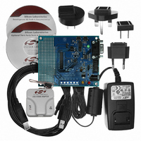
DEV KIT FOR C8051F330/F331
Manufacturer
Silicon Laboratories Inc
Type
MCUr
Specifications of C8051F330DK
Contents
Evaluation Board, Power Supply, USB Cables, Adapter and Documentation
Processor To Be Evaluated
C8051F33x
Interface Type
RS-232
Operating Supply Voltage
7 V to 15 V
Silicon Manufacturer
Silicon Labs
Core Architecture
8051
Silicon Core Number
C8051F330
Silicon Family Name
C8051F33x
Lead Free Status / RoHS Status
Contains lead / RoHS non-compliant
For Use With/related Products
Silicon Laboratories C8051F330, C8051F331
Lead Free Status / Rohs Status
Lead free / RoHS Compliant
Other names
336-1264


C8051F330/1/2/3/4/5
11.4.3. System Clock
Additional Flash recommendations and example code can be found in AN201, "Writing to Flash from Firm-
ware", available from the Silicon Laboratories web site.
108
Bits7–2: UNUSED: Read = 000000b, Write = don’t care.
Bit1:
Bit0:
Bit7
—
R
10. Make certain that the Flash write and erase pointer variables are not located in XRAM. See
11. Add address bounds checking to the routines that write or erase Flash memory to ensure that
12. If operating from an external crystal, be advised that crystal performance is susceptible to
13. If operating from the external oscillator, switch to the internal oscillator during Flash write or
viced in priority order after the Flash operation has been completed and interrupts have been
re-enabled by software.
your compiler documentation for instructions regarding how to explicitly locate variables in dif-
ferent memory areas.
a routine called with an illegal address does not result in modification of the Flash.
electrical interference and is sensitive to layout and to changes in temperature. If the system
is operating in an electrically noisy environment, use the internal oscillator or use an external
CMOS clock.
erase operations. The external oscillator can continue to run, and the CPU can switch back to
the external oscillator after the Flash operation has completed.
PSEE: Program Store Erase Enable
Setting this bit (in combination with PSWE) allows an entire page of Flash program memory
to be erased. If this bit is logic 1 and Flash writes are enabled (PSWE is logic 1), a write to
Flash memory using the MOVX instruction will erase the entire page that contains the loca-
tion addressed by the MOVX instruction. The value of the data byte written does not matter.
0: Flash program memory erasure disabled.
1: Flash program memory erasure enabled.
PSWE: Program Store Write Enable
Setting this bit allows writing a byte of data to the Flash program memory using the MOVX
write instruction. The Flash location should be erased before writing data.
0: Writes to Flash program memory disabled.
1: Writes to Flash program memory enabled; the MOVX write instruction targets Flash
memory.
SFR Definition 11.1. PSCTL: Program Store R/W Control
Bit6
—
R
Bit5
—
R
Bit4
—
R
Rev. 1.7
Bit3
—
R
Bit2
—
R
PSEE
R/W
Bit1
SFR Address:
PSWE
R/W
Bit0
0x8F
00000000
Reset Value
Related parts for C8051F330DK
Image
Part Number
Description
Manufacturer
Datasheet
Request
R

Part Number:
Description:
SMD/C°/SINGLE-ENDED OUTPUT SILICON OSCILLATOR
Manufacturer:
Silicon Laboratories Inc
Part Number:
Description:
Manufacturer:
Silicon Laboratories Inc
Datasheet:
Part Number:
Description:
N/A N/A/SI4010 AES KEYFOB DEMO WITH LCD RX
Manufacturer:
Silicon Laboratories Inc
Datasheet:
Part Number:
Description:
N/A N/A/SI4010 SIMPLIFIED KEY FOB DEMO WITH LED RX
Manufacturer:
Silicon Laboratories Inc
Datasheet:
Part Number:
Description:
N/A/-40 TO 85 OC/EZLINK MODULE; F930/4432 HIGH BAND (REV E/B1)
Manufacturer:
Silicon Laboratories Inc
Part Number:
Description:
EZLink Module; F930/4432 Low Band (rev e/B1)
Manufacturer:
Silicon Laboratories Inc
Part Number:
Description:
I°/4460 10 DBM RADIO TEST CARD 434 MHZ
Manufacturer:
Silicon Laboratories Inc
Part Number:
Description:
I°/4461 14 DBM RADIO TEST CARD 868 MHZ
Manufacturer:
Silicon Laboratories Inc
Part Number:
Description:
I°/4463 20 DBM RFSWITCH RADIO TEST CARD 460 MHZ
Manufacturer:
Silicon Laboratories Inc
Part Number:
Description:
I°/4463 20 DBM RADIO TEST CARD 868 MHZ
Manufacturer:
Silicon Laboratories Inc
Part Number:
Description:
I°/4463 27 DBM RADIO TEST CARD 868 MHZ
Manufacturer:
Silicon Laboratories Inc
Part Number:
Description:
I°/4463 SKYWORKS 30 DBM RADIO TEST CARD 915 MHZ
Manufacturer:
Silicon Laboratories Inc
Part Number:
Description:
N/A N/A/-40 TO 85 OC/4463 RFMD 30 DBM RADIO TEST CARD 915 MHZ
Manufacturer:
Silicon Laboratories Inc
Part Number:
Description:
I°/4463 20 DBM RADIO TEST CARD 169 MHZ
Manufacturer:
Silicon Laboratories Inc