C8051F330DK Silicon Laboratories Inc, C8051F330DK Datasheet - Page 114
C8051F330DK
Manufacturer Part Number
C8051F330DK
Description
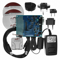
DEV KIT FOR C8051F330/F331
Manufacturer
Silicon Laboratories Inc
Type
MCUr
Specifications of C8051F330DK
Contents
Evaluation Board, Power Supply, USB Cables, Adapter and Documentation
Processor To Be Evaluated
C8051F33x
Interface Type
RS-232
Operating Supply Voltage
7 V to 15 V
Silicon Manufacturer
Silicon Labs
Core Architecture
8051
Silicon Core Number
C8051F330
Silicon Family Name
C8051F33x
Lead Free Status / RoHS Status
Contains lead / RoHS non-compliant
For Use With/related Products
Silicon Laboratories C8051F330, C8051F331
Lead Free Status / Rohs Status
Lead free / RoHS Compliant
Other names
336-1264


C8051F330/1/2/3/4/5
13.3.1. External Crystal Example
If a crystal or ceramic resonator is used as an external oscillator source for the MCU, the circuit should be
configured as shown in Figure 13.1, Option 1. The External Oscillator Frequency Control value (XFCN)
should be chosen from the Crystal column of the table in SFR Definition 13.4 (OSCXCN register). For
example, an 11.0592 MHz crystal requires an XFCN setting of 111b and a 32.768 kHz Watch Crystal
requires an XFCN setting of 001b. After an external 32.768 kHz oscillator is stabilized, the XFCN setting
can be switched to 000 to save power. It is recommended to enable the missing clock detector before
switching the system clock to any external oscillator source.
When the crystal oscillator is first enabled, the oscillator amplitude detection circuit requires a settling time
to achieve proper bias. Introducing a delay of 1 ms between enabling the oscillator and checking the
XTLVLD bit will prevent a premature switch to the external oscillator as the system clock. Switching to the
external oscillator before the crystal oscillator has stabilized can result in unpredictable behavior. The rec-
ommended procedure is:
Important Note on External Crystals: Crystal oscillator circuits are quite sensitive to PCB layout. The
crystal should be placed as close as possible to the XTAL pins on the device. The traces should be as
short as possible and shielded with ground plane from any other traces which could introduce noise or
interference.
118
Step 1. Force XTAL1 and XTAL2 to a low state. This involves enabling the Crossbar and writing ‘0’
Step 2. Configure XTAL1 and XTAL2 as analog inputs using register P0MDIN.
Step 3. Enable the external oscillator.
Step 4. Wait at least 1 ms.
Step 5. Poll for XTLVLD => ‘1’.
Step 6. Enable the Missing Clock Detector.
Step 7. Switch the system clock to the external oscillator.
to port latches P0.2 and P0.3.
Rev. 1.7
Related parts for C8051F330DK
Image
Part Number
Description
Manufacturer
Datasheet
Request
R

Part Number:
Description:
SMD/C°/SINGLE-ENDED OUTPUT SILICON OSCILLATOR
Manufacturer:
Silicon Laboratories Inc
Part Number:
Description:
Manufacturer:
Silicon Laboratories Inc
Datasheet:
Part Number:
Description:
N/A N/A/SI4010 AES KEYFOB DEMO WITH LCD RX
Manufacturer:
Silicon Laboratories Inc
Datasheet:
Part Number:
Description:
N/A N/A/SI4010 SIMPLIFIED KEY FOB DEMO WITH LED RX
Manufacturer:
Silicon Laboratories Inc
Datasheet:
Part Number:
Description:
N/A/-40 TO 85 OC/EZLINK MODULE; F930/4432 HIGH BAND (REV E/B1)
Manufacturer:
Silicon Laboratories Inc
Part Number:
Description:
EZLink Module; F930/4432 Low Band (rev e/B1)
Manufacturer:
Silicon Laboratories Inc
Part Number:
Description:
I°/4460 10 DBM RADIO TEST CARD 434 MHZ
Manufacturer:
Silicon Laboratories Inc
Part Number:
Description:
I°/4461 14 DBM RADIO TEST CARD 868 MHZ
Manufacturer:
Silicon Laboratories Inc
Part Number:
Description:
I°/4463 20 DBM RFSWITCH RADIO TEST CARD 460 MHZ
Manufacturer:
Silicon Laboratories Inc
Part Number:
Description:
I°/4463 20 DBM RADIO TEST CARD 868 MHZ
Manufacturer:
Silicon Laboratories Inc
Part Number:
Description:
I°/4463 27 DBM RADIO TEST CARD 868 MHZ
Manufacturer:
Silicon Laboratories Inc
Part Number:
Description:
I°/4463 SKYWORKS 30 DBM RADIO TEST CARD 915 MHZ
Manufacturer:
Silicon Laboratories Inc
Part Number:
Description:
N/A N/A/-40 TO 85 OC/4463 RFMD 30 DBM RADIO TEST CARD 915 MHZ
Manufacturer:
Silicon Laboratories Inc
Part Number:
Description:
I°/4463 20 DBM RADIO TEST CARD 169 MHZ
Manufacturer:
Silicon Laboratories Inc