C8051F330DK Silicon Laboratories Inc, C8051F330DK Datasheet - Page 119
C8051F330DK
Manufacturer Part Number
C8051F330DK
Description
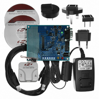
DEV KIT FOR C8051F330/F331
Manufacturer
Silicon Laboratories Inc
Type
MCUr
Specifications of C8051F330DK
Contents
Evaluation Board, Power Supply, USB Cables, Adapter and Documentation
Processor To Be Evaluated
C8051F33x
Interface Type
RS-232
Operating Supply Voltage
7 V to 15 V
Silicon Manufacturer
Silicon Labs
Core Architecture
8051
Silicon Core Number
C8051F330
Silicon Family Name
C8051F33x
Lead Free Status / RoHS Status
Contains lead / RoHS non-compliant
For Use With/related Products
Silicon Laboratories C8051F330, C8051F331
Lead Free Status / Rohs Status
Lead free / RoHS Compliant
Other names
336-1264


14. Port Input/Output
Digital and analog resources are available through 17 I/O pins. Port pins are organized as two byte-wide
Ports and one 1-bit Port. Each of the Port pins can be defined as general-purpose I/O (GPIO) or analog
input; Port pins P0.0 - P1.7 can be assigned to one of the internal digital resources as shown in
Figure 14.3. The designer has complete control over which functions are assigned, limited only by the
number of physical I/O pins. This resource assignment flexibility is achieved through the use of a Priority
Crossbar Decoder. Note that the state of a Port I/O pin can always be read in the corresponding Port latch,
regardless of the Crossbar settings.
The Crossbar assigns the selected internal digital resources to the I/O pins based on the Priority Decoder
(Figure 14.3 and Figure 14.4). The registers XBR0 and XBR1, defined in SFR Definition 14.1 and SFR
Definition 14.2, are used to select internal digital functions.
All Port I/Os are 5 V tolerant (refer to Figure 14.2 for the Port cell circuit). The Port I/O cells are configured
as either push-pull or open-drain in the Port Output Mode registers (PnMDOUT, where n = 0,1). Complete
Electrical Specifications for Port I/O are given in Table 14.1 on page 134.
Highest
Priority
Lowest
Priority
SYSCLK
Outputs
SMBus
T0, T1
UART
P0
P1
PCA
CP0
SPI
(P0.0-P0.7)
(P1.0-P1.7)
Figure 14.1. Port I/O Functional Block Diagram
2
4
2
2
4
2
8
8
Rev. 1.7
PnSKIP Registers
XBR0, XBR1,
Crossbar
Decoder
Priority
Digital
C8051F330/1/2/3/4/5
8
8
PnMDIN Registers
PnMDOUT,
Cells
Cells
I/O
I/O
P0
P1
P0.0
P0.7
P1.0
P1.7
123
Related parts for C8051F330DK
Image
Part Number
Description
Manufacturer
Datasheet
Request
R

Part Number:
Description:
SMD/C°/SINGLE-ENDED OUTPUT SILICON OSCILLATOR
Manufacturer:
Silicon Laboratories Inc
Part Number:
Description:
Manufacturer:
Silicon Laboratories Inc
Datasheet:
Part Number:
Description:
N/A N/A/SI4010 AES KEYFOB DEMO WITH LCD RX
Manufacturer:
Silicon Laboratories Inc
Datasheet:
Part Number:
Description:
N/A N/A/SI4010 SIMPLIFIED KEY FOB DEMO WITH LED RX
Manufacturer:
Silicon Laboratories Inc
Datasheet:
Part Number:
Description:
N/A/-40 TO 85 OC/EZLINK MODULE; F930/4432 HIGH BAND (REV E/B1)
Manufacturer:
Silicon Laboratories Inc
Part Number:
Description:
EZLink Module; F930/4432 Low Band (rev e/B1)
Manufacturer:
Silicon Laboratories Inc
Part Number:
Description:
I°/4460 10 DBM RADIO TEST CARD 434 MHZ
Manufacturer:
Silicon Laboratories Inc
Part Number:
Description:
I°/4461 14 DBM RADIO TEST CARD 868 MHZ
Manufacturer:
Silicon Laboratories Inc
Part Number:
Description:
I°/4463 20 DBM RFSWITCH RADIO TEST CARD 460 MHZ
Manufacturer:
Silicon Laboratories Inc
Part Number:
Description:
I°/4463 20 DBM RADIO TEST CARD 868 MHZ
Manufacturer:
Silicon Laboratories Inc
Part Number:
Description:
I°/4463 27 DBM RADIO TEST CARD 868 MHZ
Manufacturer:
Silicon Laboratories Inc
Part Number:
Description:
I°/4463 SKYWORKS 30 DBM RADIO TEST CARD 915 MHZ
Manufacturer:
Silicon Laboratories Inc
Part Number:
Description:
N/A N/A/-40 TO 85 OC/4463 RFMD 30 DBM RADIO TEST CARD 915 MHZ
Manufacturer:
Silicon Laboratories Inc
Part Number:
Description:
I°/4463 20 DBM RADIO TEST CARD 169 MHZ
Manufacturer:
Silicon Laboratories Inc