C8051F330DK Silicon Laboratories Inc, C8051F330DK Datasheet - Page 152
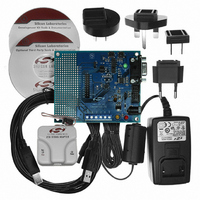
C8051F330DK
Manufacturer Part Number
C8051F330DK
Description
DEV KIT FOR C8051F330/F331
Manufacturer
Silicon Laboratories Inc
Type
MCUr
Specifications of C8051F330DK
Contents
Evaluation Board, Power Supply, USB Cables, Adapter and Documentation
Processor To Be Evaluated
C8051F33x
Interface Type
RS-232
Operating Supply Voltage
7 V to 15 V
Silicon Manufacturer
Silicon Labs
Core Architecture
8051
Silicon Core Number
C8051F330
Silicon Family Name
C8051F33x
Lead Free Status / RoHS Status
Contains lead / RoHS non-compliant
For Use With/related Products
Silicon Laboratories C8051F330, C8051F331
Lead Free Status / Rohs Status
Lead free / RoHS Compliant
Other names
336-1264


C8051F330/1/2/3/4/5
16.2.2. 9-Bit UART
9-bit UART mode uses a total of eleven bits per data byte: a start bit, 8 data bits (LSB first), a programma-
ble ninth data bit, and a stop bit. The state of the ninth transmit data bit is determined by the value in TB80
(SCON0.3), which is assigned by user software. It can be assigned the value of the parity flag (bit P in reg-
ister PSW) for error detection, or used in multiprocessor communications. On receive, the ninth data bit
goes into RB80 (SCON0.2) and the stop bit is ignored.
Data transmission begins when an instruction writes a data byte to the SBUF0 register. The TI0 Transmit
Interrupt Flag (SCON0.1) is set at the end of the transmission (the beginning of the stop-bit time). Data
reception can begin any time after the REN0 Receive Enable bit (SCON0.4) is set to ‘1’. After the stop bit
is received, the data byte will be loaded into the SBUF0 receive register if the following conditions are met:
(1) RI0 must be logic 0, and (2) if MCE0 is logic 1, the 9th bit must be logic 1 (when MCE0 is logic 0, the
state of the ninth data bit is unimportant). If these conditions are met, the eight bits of data are stored in
SBUF0, the ninth bit is stored in RB80, and the RI0 flag is set to ‘1’. If the above conditions are not met,
SBUF0 and RB80 will not be loaded and the RI0 flag will not be set to ‘1’. A UART0 interrupt will occur if
enabled when either TI0 or RI0 is set to ‘1’.
MARK
START
STOP
D0
D1
D2
D3
D4
D5
D6
D7
D8
BIT
BIT
SPACE
BIT TIMES
BIT SAMPLING
Figure 16.5. 9-Bit UART Timing Diagram
16.3. Multiprocessor Communications
9-Bit UART mode supports multiprocessor communication between a master processor and one or more
slave processors by special use of the ninth data bit. When a master processor wants to transmit to one or
more slaves, it first sends an address byte to select the target(s). An address byte differs from a data byte
in that its ninth bit is logic 1; in a data byte, the ninth bit is always set to logic 0.
Setting the MCE0 bit (SCON0.5) of a slave processor configures its UART such that when a stop bit is
received, the UART will generate an interrupt only if the ninth bit is logic 1 (RB80 = 1) signifying an address
byte has been received. In the UART interrupt handler, software will compare the received address with
the slave's own assigned 8-bit address. If the addresses match, the slave will clear its MCE0 bit to enable
interrupts on the reception of the following data byte(s). Slaves that weren't addressed leave their MCE0
bits set and do not generate interrupts on the reception of the following data bytes, thereby ignoring the
data. Once the entire message is received, the addressed slave resets its MCE0 bit to ignore all transmis-
sions until it receives the next address byte.
Multiple addresses can be assigned to a single slave and/or a single address can be assigned to multiple
slaves, thereby enabling "broadcast" transmissions to more than one slave simultaneously. The master
processor can be configured to receive all transmissions or a protocol can be implemented such that the
master/slave role is temporarily reversed to enable half-duplex transmission between the original master
and slave(s).
156
Rev. 1.7
Related parts for C8051F330DK
Image
Part Number
Description
Manufacturer
Datasheet
Request
R

Part Number:
Description:
SMD/C°/SINGLE-ENDED OUTPUT SILICON OSCILLATOR
Manufacturer:
Silicon Laboratories Inc
Part Number:
Description:
Manufacturer:
Silicon Laboratories Inc
Datasheet:
Part Number:
Description:
N/A N/A/SI4010 AES KEYFOB DEMO WITH LCD RX
Manufacturer:
Silicon Laboratories Inc
Datasheet:
Part Number:
Description:
N/A N/A/SI4010 SIMPLIFIED KEY FOB DEMO WITH LED RX
Manufacturer:
Silicon Laboratories Inc
Datasheet:
Part Number:
Description:
N/A/-40 TO 85 OC/EZLINK MODULE; F930/4432 HIGH BAND (REV E/B1)
Manufacturer:
Silicon Laboratories Inc
Part Number:
Description:
EZLink Module; F930/4432 Low Band (rev e/B1)
Manufacturer:
Silicon Laboratories Inc
Part Number:
Description:
I°/4460 10 DBM RADIO TEST CARD 434 MHZ
Manufacturer:
Silicon Laboratories Inc
Part Number:
Description:
I°/4461 14 DBM RADIO TEST CARD 868 MHZ
Manufacturer:
Silicon Laboratories Inc
Part Number:
Description:
I°/4463 20 DBM RFSWITCH RADIO TEST CARD 460 MHZ
Manufacturer:
Silicon Laboratories Inc
Part Number:
Description:
I°/4463 20 DBM RADIO TEST CARD 868 MHZ
Manufacturer:
Silicon Laboratories Inc
Part Number:
Description:
I°/4463 27 DBM RADIO TEST CARD 868 MHZ
Manufacturer:
Silicon Laboratories Inc
Part Number:
Description:
I°/4463 SKYWORKS 30 DBM RADIO TEST CARD 915 MHZ
Manufacturer:
Silicon Laboratories Inc
Part Number:
Description:
N/A N/A/-40 TO 85 OC/4463 RFMD 30 DBM RADIO TEST CARD 915 MHZ
Manufacturer:
Silicon Laboratories Inc
Part Number:
Description:
I°/4463 20 DBM RADIO TEST CARD 169 MHZ
Manufacturer:
Silicon Laboratories Inc